background image

— 57 —

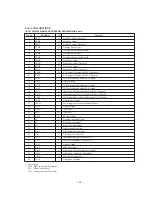
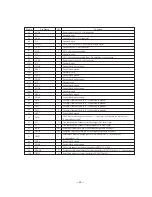
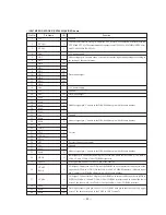
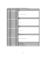
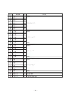
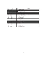
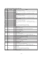
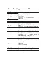
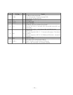
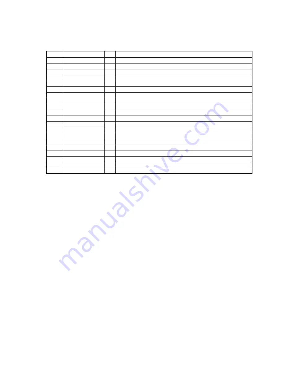
Pin Name

XRST

DIRC

SCLK

DFSW

ATSK

DATA

XLAT

CLOK

COUT

DV

DD

MIRR

DFCT

FOK

FSW

MON

NDP

MDS

LOCK

SSTP

SFDR

Pin No.

81

82

83

84

85

86

87

88

89

90

91

92

93

94

95

96

97

98

99

100

I/O

I

I

I

I

I

I

I

I

O

O

O

O

O

O

O

O

O

I

O

Abbreviation
DFCT : Defect
GFS

: Guarded Frame Sync

Function

System reset

Used in 1-track jump mode (+5v)

SENS serial data read-out clock

Defect selection pin (Ground)

Input pin for anti-shock (Ground)

Serial data input, supplied from CPU

Latch input, supplied from CPU

Serial data transfer clock input, supplied from CPU

Numbers of track counted signal output (Not used)

Digital power supply

Mirror signal output

Defect signal output

Focus OK output

Output to select spindle motor output filter (Not used)

Output to control ON/OFF of spindle motor (Not used)

Output to control spindle motor servo

Output to control spindle motor servo (Not used)

GFS is sampled by 460 Hz. H when GFS is H (Not used)

Input signal to detect disc inner most track

Sled drive output

Summary of Contents for MCE-K700

Page 1: ...1 MICROFILM MCE K700 E Model SPECIFICATIONS Model Name Using Similar Mechanism MCE F500 CD Mechanism Type CDM14 5BD21 Base Unit Type BU 5BD21 Optical Pick up Type KSS 213B SERVICE MANUAL VIDEO CD PLAYER ...

Page 2: ... 4 DISASSEMBLY 4 1 Front Panel 17 4 2 Base Unit BU 5BD21 17 5 ELECTRICAL ADJUSTMENTS 18 6 DIAGRAMS 6 1 Circuit Boards Location 20 6 2 Block Diagrams CD Main Section 21 Video Section 25 6 3 Printed Wiring Board BD Section 29 6 4 Schematic Diagram BD Section 31 6 5 Printed Wiring Board Main Displ Section 34 6 6 Schematic Diagram Main Disp Section 37 6 7 Schematic Diagram Video Section 43 6 8 Printed...

Page 3: ... on clothing and the human body During repair pay attention to electrostatic break down and also use the procedure in the printed matter which is included in the repain parts The flexible board is easily damaged and should be handled with care NOTES ON LASER DIODE EMISSION CHECK The laser beam on this model is concentrated so as to be focused on the disc reflective surface by the objective lens in...

Page 4: ...und signal can be observed at J102 AUDIO OUT using an oscilloscope 1 Turn the power on 2 Connect the SL501 C BAR on the VIDEO board with solder 3 After measuring remove the soldering installed E F BALANCE MODE Refer to SECTION 5 ELECTRICAL ADJUSTMENTS page 15 1 Turn the power on 2 Connect the SL502 and SL503 on the VIDEO board with solder 3 Press the button in playback 4 Every pressing the KARAOKE...

Page 5: ... numbers are displayed only while the corre sponding buttons are pressed 5 To exit the test mode disconnect the power plug from the outlet 7 segment display PANEL BOARD Conductor side Button Name Button Number Displayed only while a button is pressed KEY CONTROL KEY CONTROL N KEY CONTROL n KARAOKE STAR DNR OPEN CLOSE 0 SELECT POWER P Figure 9 Figure 10 Figure 11 Figure 12 Figure 13 Figure 14 Figur...

Page 6: ... MIC 1 LEVEL control 4 MIC 2 LEVEL control 5 VOCAL LEVEL control 6 Disc tray KEY CONTROL buttons 7 N button 8 button 9 n button º OPEN CLOSE button DNR button Digital Noise Reduction KARAOKE STAR button 0 button button Jog dial control JOG SELECTOR Remote sensor SELECT button p stop button ª P pause button º play button Display window KARAOKE PON button MPX button MUSIC LEVEL SWITCH LOW MID HIGH M...

Page 7: ...CT play button P pause button 0 buttons INDEX C c buttons POWER button PICTURE DNR button CONTROL COMET button TIME button Numeric buttons ª KEY CONTROL button º KEY CONTROL N button KEY CONTROL button KARAOKE PON button MPX button A B A B repeat button REPEAT A B CLEAR button p stop button PREV NEXT buttons ˆ RETURN button ª SLOW button º TV operation buttons º ª º ª 1 2 3 9 5 4 6 º 8 7 ...

Page 8: ... 8 ...

Page 9: ... 9 ...

Page 10: ... 10 ...

Page 11: ... 11 ...

Page 12: ... 12 ...

Page 13: ... 13 ...

Page 14: ... 14 ...

Page 15: ... 15 ...

Page 16: ... 16 ...

Page 17: ...e disc table will be moved Then pull out the disc table by your hand to remove the loading panel as the figure shows After that take out the front panel block SECTION 4 DISASSEMBLY 4 2 BASE UNIT BU 5BD21 Tapering driver Loading panel 1 Turn the cam to the direction of arrow counter clock wise by tapering driver BU 5BD21 2 Take off the disc table 3 Yoke bracket 4 Remove the Base unit BU 5BD21 to th...

Page 18: ... p S curve waveform symmetry within 3 1 Vp p A B 6 After check remove the lead wire connected in step 2 Note Try to measure several times to make sure than the ratio of A B or B A is more than 10 7 Take sweep time as long as possible and light up the bright ness to obtain best waveform RF Level Check Procedure 1 Connect oscilloscope to test point TP RF on BD board 2 Turned Power switch on 3 Put di...

Page 19: ...oard CHECK 13 5 MHz frequency counter VIDEO BOARD SIDE B Adjustment Location BD BOARD SIDE A 10 11 20 1 IC103 RF FEI FE TE VC PLCK IC101 2 Turned Power switch on 3 Put the disc YEDS 18 in to play the number five track Confirm that reading on frequency counter is 4 3218MHz 2 Adjust CT501 of the VIDEO board so that the frequency counter read 13 5MHz 40Hz at STOP condition GND IC512 CHECK GND CHECK 1...

Page 20: ... 20 SECTION 6 DIAGRAMS 6 1 CIRCUIT BOARDS LOCATION MIC board LOADING board JOG board MAIN board BD board DISP board VOL board PW board VIDEO board REG board TR board TRANS board ...

Page 21: ......

Page 22: ......

Page 23: ......

Page 24: ......

Page 25: ......

Page 26: ......

Page 27: ......

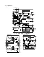
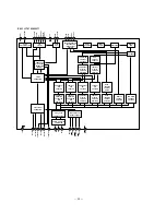
Page 28: ...GEN 37 BIAS 44 WDCK 45 LRCK 66 FSTI 82 DIRC 83 SCLK 84 DFSW 85 ATSK 98 LOCK 99 SRON SRDR 1 2 SFON SFDR 3 100 DA01 16 61 46 TFDR TFON 4 7 TRON TRDR 5 6 FFDR FFON 8 11 FRON FRDR 9 10 SSTP 16 TES2 14 TEST 17 TES3 TRACKING SERVO SLED PWM GENERATOR 2 TRACKING PWM GENERATOR FOCUS PWM GENERATOR SLED SERVO SERVO DSP PWM GENERATOR 2 2 2 2 2 93 FOK 92 DFCT 91 MIRR 80 SENS 89 COUT 88 CLOK 86 DATA 71 D OUT 79...

Page 29: ...L2 15 BSL1 16 VSS2 17 VDD1 18 AVS3 19 LO3 21 AVD3 22 AVD2 23 AVS2 26 N C 27 N C 28 AOUT2 29 AVS5 30 AIN2 24 LO2 25 AIN3 20 128K BIT DELAY RAM MICRO COMPUTER INTERFACE SERIAL DATA INTERFACE A D CONVERTER 1 A D CONVERTER 2 A D CONVERTER 3 READY 99 SCK 98 XMST 95 LRCK 94 BCK 93 SI 92 SO 91 XS24 90 VSS7 89 TST3 88 TST2 87 TST1 86 TST0 85 VDD5 84 VSS6 83 N C 82 N C 81 AVD1 50 LO1 49 N C 48 AIN1 47 AVS1...

Page 30: ... 75 74 73 72 71 70 69 68 67 66 65 64 63 62 61 VIDEO POSTPROCESSOR SYNC GENERATOR CLOCK RESET CLOCK TEST HOST INTERFACE CD ROM DECODER D RAM INTERFACE MPEG SYSTEM DECODER MPEG AUDIO DECODER MPEG VIDEO DECODER EACH CIRCUIT BLOCK 81 YUV RGB CONVERSION 80 CSYNCO 82 VSS6 83 TEST 84 TTI 85 TEN 86 TTK 87 IFSEL1 88 IFSEL2 89 NRON 90 LEVEL0 91 LEVEL1 92 VDO4 93 XRST 94 VSS7 95 CSYNCI 96 CBLNKI 97 VSYNCI 98...

Page 31: ...EST1 XTEST3 36 TD8 35 TD9 34 VDD 33 TD1O 53 VDD 54 XTEST4 55 XRST 56 SYSCLK 57 PDCLK 58 VSS 59 VSYNC 60 HSYNC 61 SO 62 FID 63 VDD 64 XIICEN 1 2 SYNC Gen and Timing Controller SIO and I2 O Bus Controller 3 8 Sub Carrier Gen Modulator Dempx Level Translator and Interpolator 4 2 2 to 4 4 4 Y C Y U V selector and Interpolator SYNC Slope Gen Closed Caption Encoder for NTSC CSYNC CHROMA V U Y BURST FLAG...

Page 32: ...ICAL DOT COUNTER FLASH INVERTER CONTROL REGISTER FLASH INVERTER CONTROL CIRCUIT DISPLAY CONTROL REGISTER RAM WRITE ADDRESS COUNTER VERTICAL DISPLAY POSITION REGISTER HORIZONTAL DISPLAY POSITION DETECTION COMPOSITE SYNC SIGNAL SEPARATION CONTROL VERTICAL DISPLAY POSITION DETECTION CHARACTER CONTROL COUNTER CHARACTER OUTPUT BACKGROUND VIDEO OUTPUT CONTROL ROW CONTROL COUNTER SHIFT REGISTER SYNC SEP ...

Page 33: ... VCO output for analog EFM PLL Not used VCO output for analog EFM PLL Ground TEST pin connected normally to Ground Digital Ground TEST pin connected normally to Ground TEST pin connected normally to Ground Charge pump output for analog EFM PLL Not used Charge pump output for variable pitch PLL Not used Clock input from variable pitch external VCO Ground Analog power supply Power supply pin for ope...

Page 34: ...hen PSSL 1 GTOP output when PSSL 0 Not used DA 10 output when PSSL 1 XUGF output when PSSL 0 Not used DA 09 output when PSSL 1 XPLCK output when PSSL 0 DA 08 output when PSSL 1 GFS output when PSSL 0 DA 07 output when PSSL 1 RFCK output when PSSL 0 DA 06 output when PSSL 1 C2PO output when PSSL 0 Not used DA 05 output when PSSL 1 XRA0F output when PSSL 0 DA 04 output when PSSL 1 MNT3 output when P...

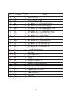
Page 35: ...Input pin for anti shock Ground Serial data input supplied from CPU Latch input supplied from CPU Serial data transfer clock input supplied from CPU Numbers of track counted signal output Not used Digital power supply Mirror signal output Defect signal output Focus OK output Output to select spindle motor output filter Not used Output to control ON OFF of spindle motor Not used Output to control s...

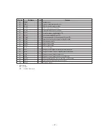
Page 36: ...nected to 5V Clock dividing output 384 768 256 512fs Frequency diving rate setting of BFOT Frequency diving rate setting of BFOT Digital block ground Digital block power supply Ground for CH 3 AD converter Analog input for CH 3 AD converter for MIC input Analog input for CH 3 AD converter OP amplifier inverter output for LPF for MIC input Power supply for CH 3 AD converter Power supply for CH 2 AD...

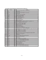
Page 37: ... open Digital block ground Digital block power supply Normally open Digital block ground Digital block power supply Test pin Normally fixed at L Connected to ground Test pin Normally fixed at L Connected to ground Test pin Normally fixed at L Connected to ground Test pin Normally fixed at L Connected to ground Digital block ground 24 32 bit slot selecting of serial data L 24 bit slot Available in ...

Page 38: ...ng tray open H open Outputs command requests to mechanism control HD6433032K07F Inputs command acknowledge from mechanism control HD6433032K07F Loading motor control Out Loading motor control In STANDBY LED lighting signal ouput H lighting POWER ON OFF control H on output A D port for MIC control input A D port 1 to 4 for key input A D port for music volume input A D port for MPX balance Echo leve...

Page 39: ...O O O O O O O Function Input output terminal exchanging data bus 0 with system controller Input output terminal exchanging data bus 1 with system controller Input output terminal exchanging data bus 2 with system controller Input output terminal exchanging data bus 3 with system controller Outputs command acknowledge to system controller Outputs command output pulses to system controller Check LED...

Page 40: ... on the address bus are valid When the read pin is Low indicates that the external addresses space is in the read state When the read pin is Low indicates that the external addresses space is in the write state and the data bus are valid Reset output Not used A D converter pin62 69 ground Test 0 input Test 1 input Test 2 input Internal state SENSE monitor input from BD boartd Audio D A converter s...

Page 41: ...t output Address signal pin Connect to the DRAM address pin with the same number Ground Address signal pin Connect to the DRAM address pin with the same number For test For test Connect to ground Ground Address signal pin Connect to the DRAM address pin with the same number RAS signal pin Connect to the RAS pin of the DRAM Same for the 256Kw 16b 256Kw 16b 2 and 512Kw 8b 2 DRAM structures WE signal...

Page 42: ...upply Ground Video output enable signal pin When set to L enables the image data output and DCLK output When set to H disables high impedance Output control can also be performed by writing in the register Output pin of the R or Cr signal of the image data MSB is R Cr7 Synchronizes with DCLK Output pin of the G orY signal of the image data MSB is G Y7 Synchronizes with DCLK 5V power supply Ground ...

Page 43: ...an input when not Signal obtained by frequency dividing the clock input from XTL0I or XTLI When the input clock is 8 fsc it can be used as the horizontal sync signal phase comparison reference signal Composite blanking signal pin Serves as an output when the built in sync generator is used and as an input when not Signal obtained by frequency dividing the clock input from XTL0I or XTLI When the in...

Page 44: ...ter access chip select signal pin Data acknowledge wait signal pin for DMA transmission register access transparent memory access Register access control signal pin Interrupt request signal Hardware reset input pin When set to L all registers and operations are reset and initialized Address input pin In some cases serves as the control signal and data input according to the setting of the control ...

Page 45: ... IC509 VIDEO PICTURE QUALITY IMPROVEMENT CXD1853Q VIDEO board Pin Name VSS BI7 BI6 BI5 BI4 BI3 BI2 BI1 BI0 VSS Y GI7 Y GI6 Y GI5 Y GI4 Y GI3 Y GI2 Y GI1 Y GI0 VSS C RI7 C RI6 C RI5 C RI4 C RI3 C RI2 C RI1 C RI0 VDD AO4 AO5 AO6 AO7 AO3 AO2 AO1 AO0 VDD XRAS XCAS XMWE Pin No 1 2 3 4 5 6 7 8 9 10 11 12 13 14 15 16 17 18 19 20 21 22 23 24 25 26 27 28 29 30 31 32 33 34 35 36 37 38 39 40 I O I I I I I I ...

Page 46: ... Pin No 41 42 43 44 45 46 47 48 49 50 51 52 53 54 55 56 57 58 59 60 61 62 63 64 65 66 67 68 69 70 71 72 73 74 75 76 77 78 79 80 I O I O I O I O I O I O I O I O I O O O O O O O O O O O O O O O O O O O O O O O O O O O O Function Ground DRAM data I O 0 7 Ground MSB R Cb Cr output 0 7 LSB Power supply 5V MSB G Y output 0 7 LSB Power supply 5V MSB B output 0 7 Open LSB Ground H SYNC output V SYNC outpu...

Page 47: ... I I I I I I I I I I I I I I Function Composit SYNC output Ground For test Connect to ground For test For test Connect to ground Matrix select RGB XYC Connect to ground System select D1851 XD1852 Connect to ground NR on off L off H on NR limitter level select 0 weak 3 strong Power supply 5V Power on reset Ground Composit SYNC input Composit blanking input V SYNC input H SYNC input Power supply 5V ...

Page 48: ... register bit PIF MODE 1 serve as input pins for multiplexed Cb Cr signals In the test mode used for internal circuit test data bus The test mode is allowed to use only for device vendors Digital ground Reference current output pin Connect a resistor 16 times 16R of the output resistance value R Voltage reference input pin Sets the output full scale value Analog power supply Analog ground 10 bit D...

Page 49: ... by Pin 64 XIICEN When the XIICEN pin is H sets into the SONY SIO mode and becomes the SCK serial clock input pin When the XIICEN pin is L sets into the I2 C BUS mode and becomes the SCL input pin The functions of this pin are selected by Pin 64 XIICEN Pulled up When the XIICEN pin is H sets into the SONY SIO mode and becomes the XCK chip select input pin When the XIICEN pin is L sets into the I2 ...

Page 50: ... When the XIICEN pin is H sets into the SONY SIO mode and becomes the S0 serial out output pin When the XIICEN pin is L this pin is not used and sets into high impedance Field ID output When control register bit FDS 1 L indicates the first field and H indicates the second field When control register bit FDS 0 H indicates the first field and L indicates the second field Digital power supply Serial ...

Page 51: ...or outputting vertical synchronizing signal Polarity can be selected metal option Not used Open Enable input pin for serial data input The serial data input becomes enable at L Incorpo rates a pull up resistor Hysteresis input Serial data input Incorporates a pull up resistor Hysteresis input Clock input pin for serial data input Incorporates a pull up resistor Hysteresis input SECAM mode select s...

Page 52: ...plied 22 22 22 22 not supplied not supplied 21 20 22 not supplied Supplied with Jack not supplied 1 1 4 984 999 01 PANEL LOADING 2 X 4947 889 1 PANEL ASSY FRONT 3 4 963 404 21 EMBLEM 5 A SONY 4 4 984 893 22 PLATE FL INDICATION 5 4 984 895 01 PLATE INDICATON 6 4 981 435 01 RING DIA 50 ORNAMENTAL 7 4 977 598 21 CUSHION 8 4 984 890 01 BUTTON TIME 9 4 984 889 21 BUTTON PLAY 10 4 984 888 11 BUTTON NR 1...

Page 53: ...ified 51 1 533 293 11 FUSE HOLDER 52 1 775 257 11 WIRE FLAT TYPE 29 CORE 53 1 775 141 11 WIRE FLAT TYPE 15 CORE 54 A 4699 505 A VIDEO BOARD COMPLETE 55 1 569 008 11 ADAPTOR CONVERSION 2P 56 3 703 244 00 BUSHING 2104 CORD 57 4 987 699 01 PANEL BACK 58 A 4699 497 A MAIN BOARD COMPLETE 59 1 664 222 11 TR BOARD 60 4 954 051 51 HOLDER PC BOARD 61 X 4947 412 1 FOOT SMALL ASSY 62 1 664 223 11 TRANS BOARD...

Page 54: ...8 11 MAGNET 102 4 933 110 41 HOLDER MG 103 4 933 112 01 TABLE DISC 104 4 967 268 01 GEAR C 105 4 927 649 01 BELT 106 4 933 107 01 GEAR PL 107 4 927 651 01 PULLEY S 108 4 933 109 01 CAM 109 1 645 721 11 LOADING BOARD 110 4 933 134 01 SCREW PTPWH M2 6X6 111 4 959 996 01 SPRING 932 COMPRESSION 112 4 933 129 01 HOLDER BU 113 4 933 111 41 CHASSIS MD 114 4 917 583 21 BRACKET YOKE 115 4 925 315 31 DAMPER...

Page 55: ...pecified Ref No Part No Description Remark Ref No Part No Description Remark 154 156 153 151 8 848 367 11 OPTICAL PICK UP BLOCK KSS 213B K N 152 1 769 069 11 WIRE FLAT TYPE 16 CORE 153 4 917 567 01 GEAR M 154 4 951 940 01 INSULATOR BU 155 4 917 565 01 SHAFT SLED 156 4 917 564 01 GEAR P FLATNESS 157 A 4673 557 A BD BOARD COMPLETE M101 X 4917 523 3 MOTOR ASSY SPINDLE M102 X 4917 504 1 MOTOR ASSY SLE...

Page 56: ... C141 1 163 038 91 CERAMIC CHIP 0 1uF 25V C151 1 163 237 11 CERAMIC CHIP 27PF 5 50V C153 1 163 038 91 CERAMIC CHIP 0 1uF 25V C154 1 164 336 11 CERAMIC CHIP 0 33uF 25V C156 1 163 237 11 CERAMIC CHIP 27PF 5 50V C157 1 163 145 00 CERAMIC CHIP 0 0015uF 5 50V C159 1 163 019 00 CERAMIC CHIP 0 0068uF 10 50V C161 1 163 038 91 CERAMIC CHIP 0 1uF 25V CONNECTOR CN101 1 774 115 11 CONNECTOR FFC FPC 29P CN102 ...

Page 57: ...ISTOR DTC114ES RESISTOR R401 1 249 429 11 CARBON 10K 5 1 4W R406 1 249 429 11 CARBON 10K 5 1 4W R407 1 249 429 11 CARBON 10K 5 1 4W R408 1 247 807 31 CARBON 100 5 1 4W R409 1 249 429 11 CARBON 10K 5 1 4W R410 1 249 429 11 CARBON 10K 5 1 4W R411 1 249 411 11 CARBON 330 5 1 4W R412 1 249 411 11 CARBON 330 5 1 4W R413 1 249 429 11 CARBON 10K 5 1 4W R414 1 249 433 11 CARBON 22K 5 1 4W R415 1 249 433 1...

Page 58: ...OAD OUT S152 1 572 086 11 SWITCH LEAF LOAD IN A 4699 497 A MAIN BOARD COMPLETE CAPACITOR C101 1 124 903 11 ELECT 1uF 20 50V C102 1 162 306 11 CERAMIC 0 01uF 30 16V C103 1 126 916 11 ELECT 1000uF 20 6 3V C104 1 130 489 00 FILM 0 0033uF 5 50V C106 1 162 306 11 CERAMIC 0 01uF 30 16V C107 1 126 233 11 ELECT 22uF 20 50V C109 1 126 022 11 ELECT 47uF 20 10V C110 1 162 306 11 CERAMIC 0 01uF 30 16V C111 1 ...

Page 59: ...22uF 25V C317 1 126 024 11 ELECT 220uF 20 25V C318 1 126 024 11 ELECT 220uF 20 25V C319 1 137 399 11 FILM 0 1uF 5 50V C320 1 137 399 11 FILM 0 1uF 5 50V CONNECTOR CN305 1 568 939 11 PIN CONNECTOR 12P CN308 1 568 936 11 PIN CONNECTOR 9P CN309 1 691 770 11 PLUG MICRO CONNECTOR 8P CN310 1 568 954 11 PIN CONNECTOR 5P DIODE D101 8 719 200 82 DIODE 11ES2 D301 8 719 200 82 DIODE 11ES2 D302 8 719 200 82 D...

Page 60: ...1 249 429 11 CARBON 10K 5 1 4W R151 1 249 441 11 CARBON 100K 5 1 4W R152 1 259 454 11 CARBON 12K 5 1 6W R153 1 259 460 11 CARBON 22K 5 1 6W R154 1 259 460 11 CARBON 22K 5 1 6W R156 1 259 466 11 CARBON 39K 5 1 6W R157 1 259 428 11 CARBON 1K 5 1 6W R158 1 259 428 11 CARBON 1K 5 1 6W R161 1 259 428 11 CARBON 1K 5 1 6W R162 1 259 452 11 CARBON 10K 5 1 6W R163 1 259 466 11 CARBON 39K 5 1 6W R165 1 259 ...

Page 61: ...04 8 719 987 63 DIODE 1N4148M D705 8 719 987 63 DIODE 1N4148M D706 8 719 987 63 DIODE 1N4148M GROUND TERMINAL EB701 1 537 770 21 TERMINAL BOARD GROUND IC IC701 8 759 503 91 IC TL082ACP IC702 8 759 710 59 IC NJM4580D D IC703 8 759 710 59 IC NJM4580D D IC704 8 759 710 59 IC NJM4580D D JACK J701 1 764 188 11 JACK SMALL TYPE DIA 3 5 MIC CONTROL J702 1 770 222 31 JACK LARGE TYPE MIC 2 J703 1 770 222 31...

Page 62: ...LE POWER 1 664 995 11 REG BOARD CAPACITOR C322 1 137 399 11 FILM 0 1uF 5 100V C323 1 136 233 11 ELECT 22 20 50V IC IC305 8 759 231 53 IC TA7805S 1 664 222 11 TR BOARD TRANSISTOR Q301 8 729 141 83 TRANSISTOR 2SB1094 LK 1 664 223 11 TRANS BOARD 1 533 293 11 FUSE HOLDER CAPACITOR C344 1 115 992 11 FILM 1uF 5 100V C910 1 128 576 11 ELECT 100uF 20 63V C911 1 126 059 11 ELECT 10uF 20 50V C912 1 162 306 ...

Page 63: ...uF 25V C583 1 163 038 91 CERAMIC CHIP 0 1uF 25V C584 1 163 038 91 CERAMIC CHIP 0 1uF 25V C585 1 163 038 91 CERAMIC CHIP 0 1uF 25V C589 1 163 038 91 CERAMIC CHIP 0 1uF 25V C590 1 163 038 91 CERAMIC CHIP 0 1uF 25V C591 1 163 038 91 CERAMIC CHIP 0 1uF 25V C592 1 126 206 11 ELECT CHIP 100uF 20 6 3V C593 1 126 206 11 ELECT CHIP 100uF 20 6 3V C594 1 163 038 91 CERAMIC CHIP 0 1uF 25V C595 1 163 038 91 CE...

Page 64: ...CHIP 10K 5 1 10W R511 1 216 025 91 METAL GLAZE 100 5 1 10W R512 1 216 049 91 METAL GLAZE 1K 5 1 10W R513 1 216 025 91 METAL GLAZE 100 5 1 10W R514 1 216 073 00 METAL CHIP 10K 5 1 10W R515 1 216 025 91 METAL GLAZE 100 5 1 10W R516 1 216 025 91 METAL GLAZE 100 5 1 10W R517 1 216 025 91 METAL GLAZE 100 5 1 10W R518 1 216 025 91 METAL GLAZE 100 5 1 10W R519 1 216 073 00 METAL CHIP 10K 5 1 10W R520 1 2...

Page 65: ...TAL 27MHz X503 1 767 361 11 VIBRATOR CERAMIC 28 6MHz X504 1 767 055 11 VIBRATOR CERAMIC 45MHz 1 664 221 11 VOL BOARD CAPACITOR C728 1 137 368 11 FILM 0 0047uF 5 50V C732 1 137 368 11 FILM 0 0047uF 5 50V RESISTOR R726 1 249 437 11 CARBON 47K 5 1 4W R741 1 249 429 11 CARBON 10K 5 1 4W R742 1 249 433 11 CARBON 22K 5 1 4W VARIABLE RESISTOR RV702 1 225 407 11 RES VAR 50K VOCAL LEVEL RV703 1 225 406 11 ...

Page 66: ... 88 MCE K700 9 960 824 11 Sony Corporation Home A V Products Company 96K097012 1 Printed in Singapore 1996 11 Published by Service and Safety Engineering Dept Shibaura ...

Reviews: