— 66 —
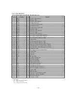
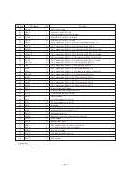
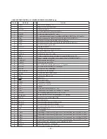
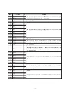
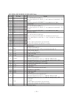
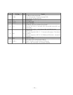
Pin Name
DATI
BCKI
DOIN
XHCS
XHDT
HRW
XHIRQ
XRST
HA0
HA1
Pin No.
111
112
113
114
115
116
117
118
119
120
I/O
I
I
I
I
I/O
I
O
I
I
I
Function
Serial data input
Bit clock input
Digital input signal
Register access chip select signal pin.
Data acknowledge/wait signal pin for DMA transmission, register access, transparent
memory access.
Register access control signal pin.
Interrupt request signal
Hardware reset input pin. When set to ‘L’, all registers and operations are reset and initialized.
Address input pin. In some cases, serves as the control signal and data input according to
the setting of the control mode.
Summary of Contents for MCE-K700
Page 8: ... 8 ...
Page 9: ... 9 ...
Page 10: ... 10 ...
Page 11: ... 11 ...
Page 12: ... 12 ...
Page 13: ... 13 ...
Page 14: ... 14 ...
Page 15: ... 15 ...
Page 16: ... 16 ...
Page 21: ......
Page 22: ......
Page 23: ......
Page 24: ......
Page 25: ......
Page 26: ......
Page 27: ......

