UP-3301US
CIRCUIT DESCRIPTION
– 60 –
10. WAIT control
The wait control function is built in the MPCA8 and is used to provide an interface with low-speed devices.
10-1. Block diagram
The block diagram of the wait control function is shown.
Fig. 10
In the figure, the decoder, wait enabling register, AND-OR sections are
the same as those in the MPCA6 or 7, but other components are newly
incorporated in the MPCA7.
EXWAITZ and WAITZ are external wait signals which are to be read
inside the MPCA8 and output to the WAITZ. The EXWAITZ is a gen-
eral-purpose wait request terminal, and WAITZ is the wait request sig-
nal from the VGA controller.
11. CKDC9
The UP-3301 performs the following controls, using the CKDC9.
• Customer display
• Clock
• Buzzer
• System reset
11-1. Interface
CKDC9 is connected through the MPCA8.
Fig. 11
12. Option RAM interface
12-1. Interface
The expanded RAM connector terminals are shown in the table.
The 72 pin S.O. DIMM is used for the connector.
Extension RAM connector terminals
ADDRESS
DECODER
RAS
ROS
IO
X3
WAIT
ENABLE
REGS.
ENABLE
1WAIT
2WAIT
3WAIT
WAIT PULSE
GENERATOR
ADDRESS
DATA
WAIT
CONTROL
REGS.
EXWAITZ
VWAITZ
S
E
L
E
C
T
O
R
WAITZ
<00FF8Dh>
<00FF8Fh>
DATA
TXD2(P87)
SCK2(P83)
RXD2(P84)
IRQ0
RES
STOP
(P57) FT12
HTS
SCK
STH
TXD1
SCL1
RXD1
IRQ0
HTS1
SCK1
STH1
INT1
RESET
HTS
SCK
STH
KRQ
SHEN
SRES
STOP
SW
RESET
RESET
H8/510
MPCA8
Standard
CKDC9
Signal
Name
Pin No.
Signal
Name
Pin No.
Signal
Name
Pin No.
GND
1
–
25
D9
49
GND
2
–
26
D8
50
–
3
–
27
D7
51
–
4
–
28
D6
52
–
5
A13
29
D5
53
–
6
A12
30
D4
54
–
7
A11
31
D3
55
–
8
A10
32
D2
56
–
9
A9
33
D1
57
–
10
A8
34
D0
58
A14
11
A7
35
GND
59
A15
12
A6
36
NC
60
A16
13
A5
37
OWR
61
A17
14
A4
38
–
62
A18
15
A3
39
–
63
A19
16
A2
40
–
64
–
17
A1
41
–
65
PCE22_E
18
A0
42
–
66
PCE21_E
19
D15
43
HWR
67
–
20
D14
44
–
68
RD
21
D13
45
VMEM
69
PCE22_O
22
D12
46
VMEM
70
PCE21_O
23
D11
47
GND
71
GND
24
D10
48
GND
72
Summary of Contents for UP-3301
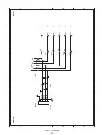
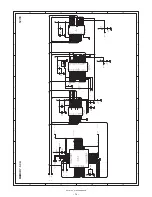
Page 91: ...UP 3301US PWB LAYOUT 89 CHAPTER 9 PWB LAYOUT 1 MAIN PWB A side ...
Page 92: ...UP 3301US PWB LAYOUT 90 B side 8 CUSTOMER DISPLAY PWB ...
Page 93: ...UP 3301US PWB LAYOUT 91 2 IR PWB 3 LCD PWB A Side B Side 4 INVERTER PWB A Side B Side ...
Page 94: ...UP 3301US PWB LAYOUT 92 5 MOTHER PWB 6 N F PWB 7 TOUCH PANEL PWB ...
Page 95: ...UP 3301US PWB LAYOUT 93 ...
Page 111: ......


