UP-3301US
CIRCUIT DESCRIPTION
– 45 –
2-4. TCP/IP Interface
1. GENERAL DESCRIPTION
The Ethernet control supports the TCP/IP protocol.
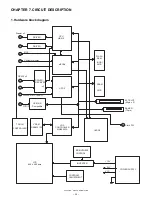
2. BLOCK DIAGRAM
*
When writing data into FLASH, switch /CS0to EP-ROM and /CS3 to
FLASH Memory.
3. CONFIGURATION
1
1
1
1
CPU : [HitachiSH-2 Series SH7014 (20MHz)]
External memory spaces, CS0 - CS3 and the DRAM space are pro-
vided. This board assigns FLASH Memory to CS0, SRAM to CS1, dual-
port SRAM to CS2, and LAN controller to CS3.
2
2
2
2
LAN Controller : [RealtekRTL8019AS (20MHz)]
The LAN controller is assigned to the CS space.
Because of the pseudo ISA connection, each register is assigned to
addresses of H00C00300 and after.
3
3
3
3
ROM (FLASH Memory) : [SharpLH28F004BVT(4Mbits)]
<Access Time = 90ns>
The ROM (FLASH Memory) is assigned to CS0 space.
Data is written onto FLASH Memory from UV-EPROM by switching the
CSO space to UV-EPROM and the CS3 space to FALSH Memory.
The MAC Address is written on FLASH Memory.
• The company code is assigned to “08001FH”.
• The serial number and adjustment byte are stored in an area of 4
bytes from the address H’0007C000.
4
4
4
4
RAM : [S-RAM 1Mbits] <Access Time=70ns>
Assigned to the CS1 space.
[IDT Dual-Port SRAM IDT7134] <Access Time=55ns>
Assigned to the CS2 space.
The IDT7134 does not have any busy signal, access to the same
address from both sides is inhibited.
5
5
5
5
Pulse Trans : [Pulse78Z034]
Is used for the 10Base-T standard and has a choke coil built in at the
output side.
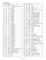
132
TRNDTC
TXD3
O
RS-232 transmission data
signal
133
/DTRC
/DTR3
O
RS-232 data terminal ready
signal
134
/RTSC
/RTS3
O
USART_C request to send
135
RCVDTC
RCVDT3
IS
RS-232 reception data sig-
nal
136
/CTSC
GND
IS
GND
137
/DSRC
/DSR3
IS
RS-232 data set ready sig-
nal
138 TRNRDYC
TRNRDY3
O
RS-232 data transmission
enable signal
139 RCVRDYC
RCVRDY3
O
RS-232 data reception
enable signal
140 TRNEMPC
TRNEMP3
O
RS-232 transmission buffer
empty signal
141
SYCBKC
NC
IO
NC
142
VCC
VCC
+5V
143
GND
GND
GND
144
/CSD
VCC
IS
USART_D chip select
145
TRNDTD
NC
O
NC
146
/DTRD
NC
O
NC
147
/RTSD
NC
O
NC
148
RCVDTD
GND
IS
GND
149
/CTSD
GND
IS
GND
150
/DSRD
GND
IS
GND
151 TRNRDYD
NC
O
NC
152 RCVRDYD
NC
O
NC
153 TRNEMPD
NC
O
NC
154
SYCBKD
NC
IO
NC
155
/WIN
/WRH
I
Write signal
156
/RIN
/RDH
I
Read signal
157
RSLCT0
AH0
I
Address bus
158
RSLCT1
AH1
I
Address bus
159
RST
RES USART
IS
Reset signal
160
MCLK
CLK USART
I,
I
TTL input
ID
TTL input with pull down
IS
TTL Schmidt input
ISU
TTL Schmidt input with pull up
IO
TTL I/O
3S
3-state Buffer (6mA)
ON6
Open drain (6mA)
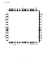
Pin
NO.
Name
UP-3301
I/O
Description
Dual-Port
RAM
4k byte
CN
RJ-45
Data Bus
Address Bus
Da
ta
Bus
LOGIC
/CS1
/CS2
/INTHR
/INTHW
/INTSR
/INTSW
10MHz
/CS0
/CS0
/CS3
/CS3
/CS2
/CS1
/CS0
/HWACK
/HRACK
/SWRQ
/SRRQ
CPU
(SH-2)
/DPCS,
/WR,/RD
Address
Bus
LD0~LD7
LA0~LA11
FLASH
512k byte
LD0~LD7
LA0~LA18
LD0~LD7
LA0~LA18
SRAM
128k byte
LD0~LD7
LA0~LA19
LD0~LD7
LA0~LA18
LAN Cnt.
(8bit-Bus)
EP-ROM
(Writing in
to FLASH)
512k byte
Summary of Contents for UP-3301
Page 91: ...UP 3301US PWB LAYOUT 89 CHAPTER 9 PWB LAYOUT 1 MAIN PWB A side ...
Page 92: ...UP 3301US PWB LAYOUT 90 B side 8 CUSTOMER DISPLAY PWB ...
Page 93: ...UP 3301US PWB LAYOUT 91 2 IR PWB 3 LCD PWB A Side B Side 4 INVERTER PWB A Side B Side ...
Page 94: ...UP 3301US PWB LAYOUT 92 5 MOTHER PWB 6 N F PWB 7 TOUCH PANEL PWB ...
Page 95: ...UP 3301US PWB LAYOUT 93 ...
Page 111: ......


