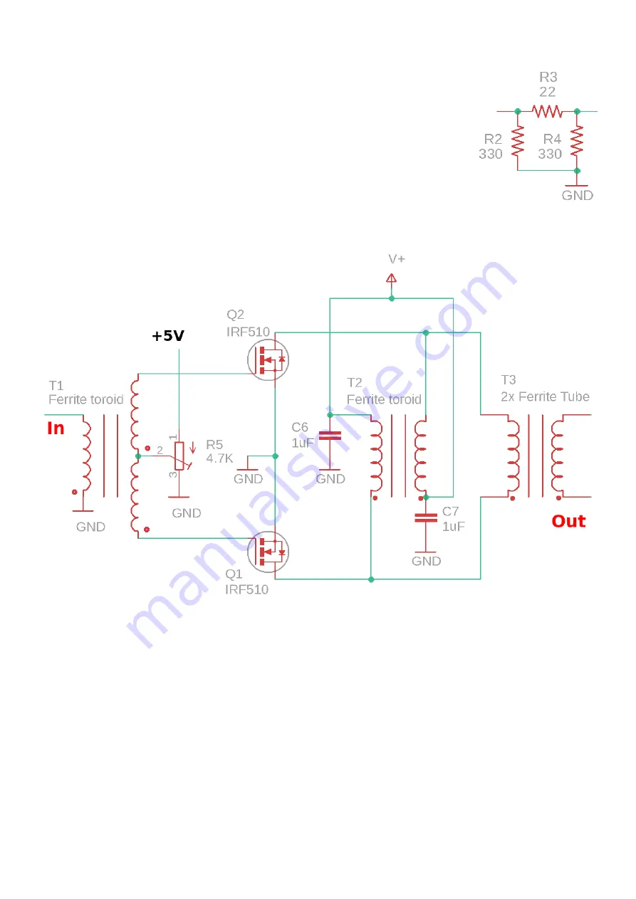
6.2 Input attenuator
The pi-network consisting of R2, R3 and R4 forms an attenuator. This is
necessary because the output of the QCX will be approximately 5W into 50-
ohms; this is a sinewave with 45V peak-peak. This will be too high for the
Gate-Source voltage specification (+/- 20V) of the IRF510 transistors.
To operate the transistor gates safely, and to correctly load the QCX at
approximately 50-ohms output impedance, and to ensure stability, this “3dB
pad” is a good practice inclusion in the circuit.
6.3 Power Amplifier
The power amplifier is a quite standard push-pull circuit consisting of two IRF510 power
MOSFETs in push-pull configuration.
DC power is supplied to the transistor drains via transformer T2 which is bifilar wound on a ferrite
toroid.
The RF output is taken via power combiner and impedance matching transformer T3, which is
wound on a pair of large ferrite tubes. The choice of turns ratio is an important design parameter
and will be discussed a little later in this section.
Input transformer T1 is trifilar-wound on a ferrite toroid. Its purpose is to split the incoming signal
into two equal and opposite parts. Each of the power transistors Q1 and Q2 will be active
(switched ON) in opposite halfs of the RF cycle. These two outputs drive the MOSFET gates
directly.
50W QCX PA kit assembly
1.00q
44


