PDP-425CMX
147
5
6
7
8
5
6
7
8
C
D
F
A
B
E
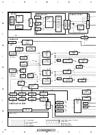
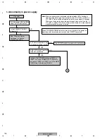
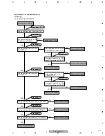
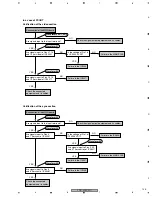
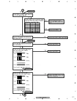
In a case when no image from any input appears
Examination of the MAIN board
Failure in the power supply
unit, or PN1 cable broken
NO
YES
YES
YES
NO
Is a CLK signal input to Pin 12 of
IC8501? And are sync signals
input to Pins 55 and 57?
Is a DE signal input to Pin 58?
YES
YES
Is the voltage at Pin 51 of
IC8501 3.3 V DC?
Disconnect the cable from the
PN1 connector. Check if 3.3V
DC is output from Pin 1 of PN1.
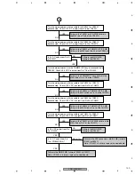
Disconnect the cable from the
PN2 connector. Check if 2.5V
DC is output from Pin 1 of PN2.
Failure in the power supply
unit, or PN2 cable broken
NO
NO
NO
NO
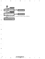
Is the voltage at Pin 1 of PN2
connector 2.5 V DC?
YES
Is the voltage at Pin 4 of
IC8002 1.5 V DC?
Failure in the MAIN PWB
Failure in the MAIN PWB
Failure in the MAIN PWB
YES
NO
YES
Is the voltage at Pin 5 of
IC8003 1.5 V DC?
NO
YES
Is a CLK signal input to Pin 3
of X8001?
Is a CLK signal input to Pin 3
of X8002?
NO
YES
YES
Failure in the IC8501
NO
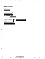
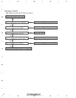
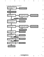
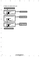
• Reset discharge is occurred.
• Mask is displayed.
• DSD is not displayed.
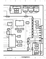
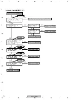
Diagnosis of Panel Module
Failure in the IC8002
Failure in the IC8003
Failure in the X8001
Failure in the X8002
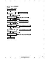
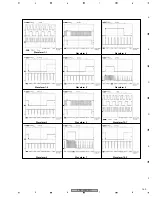
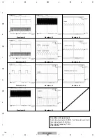
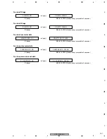
Waveform 33
Waveform 34
Waveform 35
Summary of Contents for PDP-42MXE10
Page 9: ...PDP 425CMX 9 5 6 7 8 5 6 7 8 C D F A B E ...
Page 27: ...PDP 425CMX 27 5 6 7 8 5 6 7 8 C D F A B E ...
Page 37: ...PDP 425CMX 37 5 6 7 8 5 6 7 8 C D F A B E ...
Page 129: ...PDP 425CMX 129 5 6 7 8 5 6 7 8 C D F A B E ...
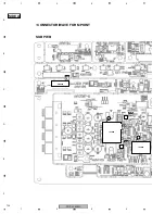
Page 132: ...PDP 425CMX 132 1 2 3 4 1 2 3 4 C D F A B E MAIN PWB CONNECTOR WAVE FORM POINT SIDE B ...

