PDP-425CMX
143
5
6
7
8
5
6
7
8
C
D
F
A
B
E
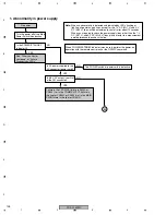
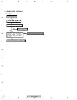
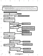
No image
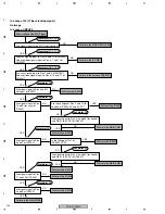
In a case of INPUT3 and INPUT4
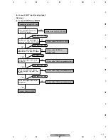
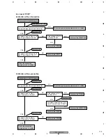
In a case of SLOT input (analog signal)
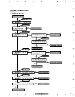
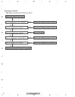
Examination of the SLOT input
Failure in the MAIN PWB
Does not either of INPUT3
or INPUT4 display?
NO
NO
NO
Failure in the VIDEO SLOT PWB
Failure in the VIDEO SLOT PWB
YES
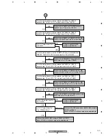
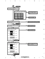
Are the sync and clock signals
output from VIDEO SLOT PWB?
NO
NO
NO
NO
YES
Failure in the I/F PWB or
flexible cable
Are the sync and clock signals
input to pins 1, 2 and 4 of CN6301?
YES
Failure in the IC6302 and peripheral parts
Failure in the IC6301 and peripheral parts
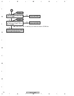
Failure in the IC6304 and peripheral parts
Is the clock signal input to pin 2
of IC6302?
YES
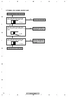
Are the sync and clock signals
input to pins 168, 169 and 172 of
IC6301?
YES
Is the clock signal input to pin 2
of IC6304?
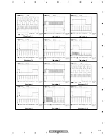
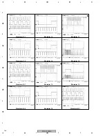
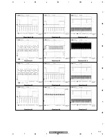
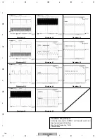
Waveform 29-1, 29-2
Waveform 29-1, 29-2
Waveform 29-1, 29-2
Waveform 29-1, 29-2
Waveform 29-2
Summary of Contents for PDP-42MXE10
Page 9: ...PDP 425CMX 9 5 6 7 8 5 6 7 8 C D F A B E ...
Page 27: ...PDP 425CMX 27 5 6 7 8 5 6 7 8 C D F A B E ...
Page 37: ...PDP 425CMX 37 5 6 7 8 5 6 7 8 C D F A B E ...
Page 129: ...PDP 425CMX 129 5 6 7 8 5 6 7 8 C D F A B E ...
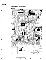
Page 132: ...PDP 425CMX 132 1 2 3 4 1 2 3 4 C D F A B E MAIN PWB CONNECTOR WAVE FORM POINT SIDE B ...


