background image

PDP-425CMX

102

1

2

3

4

1

2

3

4

C

D

F

A

B

E

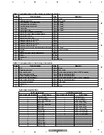
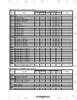
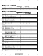
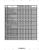
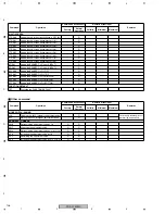
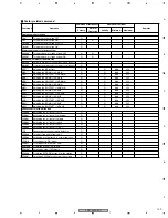
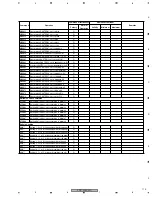
Command

Operation

Command Effectiveness

Numeric Direct input

Remarks

Factory

Normal 

Operation

Validity

Minimum

Maximum

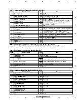
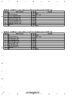
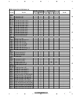
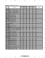
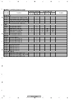
FUNCTIONAL LOCK

FCLS00

Cancelling the functional lock

-

O

-

-

-

FCLS01

Prohibiting the button operation of the main unit

-

O

-

-

-

FCLS02

Prohibiting the button operation of the remote controller

-

O

-

-

-

FCLS03

Prohibiting the button operation of the main unit and remote controller

-

O

-

-

-

FCLS04

Setting the memory lock

-

O

-

-

-

OSD

DOF

Erasing the currently OSD displyed indications

O

O

-

-

-

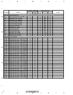
DISPLAY CALL

DITS01

Displaying the DISPLAY CALL 1

O

O

-

-

-

DITS02

Displaying the DISPLAY CALL 2

O

O

-

-

-

IM0***

Writing the INFORMATION (1-3 characters)

O

O

-

-

-

IM1***

Writing the INFORMATION (4-6 characters)

O

O

-

-

-

IM2***

Writing the INFORMATION (7-9 characters)

O

O

-

-

-

IM3***

Writing the INFORMATION (10-12 characters)

O

O

-

-

-

IM4***

Writing the INFORMATION (13-15 characters)

O

O

-

-

-

IM5***

Writing the INFORMATION (16-18 characters)

O

O

-

-

-

IM6***

Writing the INFORMATION (19-21 characters)

O

O

-

-

-

IMD

Clearing the INFORMATION

O

O

-

-

-

Summary of Contents for PDP-42MXE10

Page 1: ...LECT DOWN UP LEFT RIGHT EXIT VOLUME PDP 425CMX ARP3340 PLASMA DISPLAY PDP 425CMX PDP 42MXE10 THIS MANUAL IS APPLICABLE TO THE FOLLOWING MODEL S AND TYPE S This service manual should be used together with the following manual s Model Type Power Requirement Remarks PDP 425CMX LUC5 AC100 120V PDP 42MXE10 LDFK5 AC100 240V PDP 42MXE10 YVXK5 AC100 240V Model No Order No Remarks PDP 425CMX PDP 42MXE10 AR...

Page 2: ...be put back in place such as barriers nonmetallic knobs adjustment and compartment covershields isolation resistor capacitor etc 3 When service is required observe the original lead dress Extra precaution should be taken to assure correct lead dress in the high voltage circuitry area 4 Always use the manufacture s replacement components Especially critical components as indicated on the circuit di...

Page 3: ...c Any current measured must not exceed 0 5mA ANY MEASUREMENTS NOT WITHIN THE LIMITS OUTLINED ABOVE ARE INDICATIVE OF A POTENTIAL SHOCK HAZARD AND MUST BE CORRECTED BEFORE RETURNING THE SET TO THE CUSTOMER PRODUCT SAFETY NOTICE Many electrical and mechanical parts in PIONEER set have special safety related characteristics These are often not evident from visual inspection nor the protection afforde...

Page 4: ...r Switch S1 4 Fuse In the POWER SUPPLY Unit 5 STB Transformer and Converter Transformer In the POWER SUPPLY Unit 6 Other primary side of the POWER SUPPLY Unit High Voltage Generating Point The places where voltage is 100V or more except for the charged places described above If the places are touched there is a risk of electric shock If the procedures described in 7 1 4 POWER ON OFF FUNCTION FOR T...

Page 5: ... the product Please check that neither solder debris nor screws remain inside the product 8 There should be no semi broken wires scratches melting etc on the coating of the power cord Damaged power cords may lead to fire accidents so please be sure that there are no damages If you find a damaged power cord please exchange it with a suitable one 9 There should be no spark traces or similar marks on...

Page 6: ...DIO and SUS COMM IF ASSYS 36 3 9 POWER BLOCK DIAGRAM 38 3 10 CONNECTOR PIN DESCRIPTION 40 5 PCB PARTS LIST 56 6 ADJUSTMENT 69 6 1 ADJUSTMENT REQUIRED WHEN THE SET IS REPAIRED OR REPLACED 69 6 2 ADJUSTMENT 70 6 3 SERVICE MENU LIST 73 6 4 SERVICE MENU 74 6 5 FACTORY MODE 76 6 6 RS 232C C0MMAND 87 6 7 METHOD FOR REPLACING THE SERVICE PANEL ASSY 115 7 GENERAL INFORMATION 121 7 1 DIAGNOSIS 121 7 1 1 PC...

Page 7: ... p 75 negative sync Compatible with Microsoft Plug Play VESA DDC1 2B Output Mini D sub 15 pin socket connector 75Ω with buffer INPUT2 Input DVI D 24 pin connector Digital RGB signal DVI compliant TMDS signal Compatible with Microsoft Plug Play VESA DDC 2B Audio Input AUDIO INPUT for INPUT1 Stereo mini jack L R 500 mVrms more than 10 kΩ AUDIO INPUT for INPUT2 Stereo mini jack L R 500 mVrms more tha...

Page 8: ...errite cores x 3 for audio cables 8 Display stands x 2 9 Washers x 2 0 Hex hole bolts x 2 Remote control unit holder Cable ties x 2 These Operating Instructions Warranty Use as a holder for the remote control unit When attaching to the rear of the main unit be careful not to cover the vents ADG1215 CTX1054 AMR3545 WB80FTC SMZ80H400FTC AMR3268 AEC 093 AXD1528 AED1285 AEC2051 ATX1031 ...

Page 9: ...PDP 425CMX 9 5 6 7 8 5 6 7 8 C D F A B E ...

Page 10: ...of the part Therefore when replacing be sure to use parts of identical designation Screws adjacent to mark on product are used for disassembly For the applying amount of lubricants or glue follow the instructions in this manual In the case of no amount instructions apply as you think it appropriate NOTES 23 22 35 33 30 29 18 Except PDP 42MXE10 YVXK5 36 27 28 31 26 32 1 PDP 425CMX only 4 21 9 2 8 2...

Page 11: ...ontrast table 2 33 Reinforce Pad FT See Contrast table 2 34 Carton 42FT See Contrast table 2 35 Upper Carton See Contrast table 2 36 Mirror Mat See Contrast table 2 37 Plasma Caution Sheet See Contrast table 2 38 Image Caution Sheet See Contrast table 2 39 Image Stick Caution Sheet See Contrast table 2 Mark No Description Part No Mark No Symbol and Description PDP 425CMX LUC5 PDP 42MXE10 LDFK5 PDP...

Page 12: ...D F A B E 2 2 FRONT and REAR SECTION 3 3 16 13 1 7 15 21 21 22 22 22 22 22 22 22 22 19 22 22 22 22 22 22 22 22 22 22 22 22 22 22 22 22 22 22 22 22 18 22 12 22 5 5 6 11 8 22 9 10 17 21 21 22 3 3 3 3 3 3 14 3 3 22 4 2 3 PDP 425CMX only ...

Page 13: ...MX See Contrast table 2 12 Caution Label See Contrast table 2 13 Front Case Assy 425CMX AMB2885 14 Filter FT AMR3510 15 Control Button CMX AAC1559 16 Pioneer Badge AAM1101 17 Control Cover CMX AMR3512 18 Rear Case ANE1650 19 Bottom Cover CMX ANG2860 20 21 Screw ABZ30P100FTB 22 Screw AMZ30P060FTB Mark No Symbol and Description PDP 425CMX LUC5 PDP 42MXE10 LDFK5 PDP 42MXE10 YVXK5 NSP 6 Name Label CMX...

Page 14: ...3 15 43 43 5 28 5 28 5 28 5 28 5 28 5 28 5 28 5 28 5 28 28 18 32 10 11 12 37 37 29 43 43 43 43 43 43 20 31 32 32 29 17 43 43 42 42 22 7 6 41 41 43 44 45 16 38 27 34 23 36 8 4 9 1 43 42 26 43 29 14 33 33 29 42 24 25 19 2 43 30 43 43 43 30 30 43 21 43 35 3 13 40 40 28 39 38 38 38 45 ...

Page 15: ... ADX3284 17 Housing Wire J210 ADX3285 18 13P Housing Wire J218 ADX3286 19 COMM Bracket CMX ANG2857 20 Terminal Panel AC CMX ANG2863 21 Terminal Panel COMM CMX ANG2874 22 AC Bracket CMX Assy ANG2901 NSP 23 Audio Heatsink ANH1648 24 Slot Spring T94 ABK1034 25 Slot Spring B92 ABK1035 26 COMM I F Bracket CMX ANG2859 27 Inlet Cover XM4 ANG2899 28 Nyron Binder AEC 093 29 Wire Saddle AEC1745 30 Mini Clam...

Page 16: ...1 2 3 4 1 2 3 4 C D F A B E 2 4 MULTIBASE SECTION 21 1 16 17 23 23 23 23 17 3 6 3 19 19 19 15 7 5 18 23 23 24 21 21 21 14 14 14 14 14 14 14 4 13 13 13 13 13 10 9 21 21 21 21 8 21 11 22 22 22 22 22 22 21 3 24 24 2 12 ...

Page 17: ... or ADX3289 7 Multi Base CMX ANA1901 8 Terminal Panel MAIN CMX Assy ANG2871 9 Slot Spring T130 ABK1032 10 Slot Spring B126 ABK1033 11 Slot Panel 262 N ANG2610 12 VIDEO I F Bracket ANG2858 13 Wire Saddle AEC1745 14 Wire Saddle AEC1797 15 PCB Support AEC1958 16 Rivet AMR1066 17 VIDEO Guide Rail AMR3485 18 VIDEO I F Sheet AMR3495 19 PWB Sleeve AMR3518 20 21 Screw AMZ30P060FTB 22 Hex Head Screw BBA105...

Page 18: ...ION 5 16 3 1 20 30 31 31 29 29 17 23 31 31 31 8 31 31 31 31 31 31 17 24 7 17 13 17 17 17 17 29 29 28 28 28 28 31 31 12 6 19 31 31 28 28 28 10 11 28 31 25 25 9 31 31 31 31 31 19 19 19 31 17 17 18 18 19 19 19 17 14 31 22 21 26 30 15 30 22 21 26 30 15 20 20 20 ...

Page 19: ...926 11 Front Chassis LB FT ANA1928 12 Front Chassis B CMX ANA1933 13 Sub Frame L Assy CMX ANG2875 14 Sub Frame R Assy CMX ANG2876 15 Fan Angle FT ANG2909 16 Nyron Binder AEC 093 17 Wire Saddle AEC1745 18 Wire Saddle AEC1751 19 Mini Clamp AEC1805 20 PCB Spacer AEC1941 21 Cushion A AED1293 22 Cushion B AED1294 23 Duct Sheet L FT AMR3515 24 Duct Sheet R FT AMR3532 25 Gasket ANK1823 26 Fan Motor 80 x ...

Page 20: ...25CMX 20 1 2 3 4 1 2 3 4 C D F A B E 2 6 DRIVE SECTION 23 8 1 6 16 9 22 22 22 23 23 13 23 23 23 23 23 7 22 10 18 18 12 23 23 22 23 22 22 22 22 22 22 22 23 23 2 3 18 18 18 18 11 18 18 18 18 18 23 5 19 20 14 4 ...

Page 21: ...Ferrite Core ATX1039 7 4P Housing Wire J101 ADX3192 8 6P Housing Wire J102 ADX3193 9 3P Housing Wire J103 ADX3194 10 8P Housing Wire J105 ADX3196 11 14P Housing Wire J106 ADX3292 12 5P Housing Wire J108 ADX3199 13 9P Housing Wire J104 ADX3278 14 6P Housing Wire J107 ADX3280 15 16 Nyron Binder AEC 093 17 18 Locking Wire Saddle AEC1992 19 HS Sheet S FT AMR3519 20 HS Sheet L FT AMR3520 21 22 Screw PM...

Page 22: ...ION 9 10 13 11 12 5 17 8 7 6 6 6 6 13 13 14 16 16 16 16 16 16 16 16 15 15 16 20 13 13 18 1 3 17 16 16 16 16 16 16 16 16 16 19 16 14 14 14 14 16 16 14 14 14 16 14 20 20 2 4 4 4 4 Note The parts of encircled number denote measuring component of PDP Service Assy ...

Page 23: ...rotect Sheet FT AMR3525 20 Harness Lifter 18 AEC1980 Mark No Description Part No Mark No Symbol and Description PDP 425CMX LUC5 PDP 42MXE10 LDFK5 PDP 42MXE10 YVXK5 NSP 1 Panel Chassis FT Assy AWU1136 AWU1136 AWU1151 Mark No Description Part No PDP Service Assy 42H6D1 AWU1160 NSP Panel Chassis FT Assy AWU1136 Wire Saddle AEC1745 x5 Flat Clamp AEC1879 x9 PCB Support AEC1938 x2 PCB Spacer AEC1941 x22...

Page 24: ... 29 22 GND 30 21 VYOBI1 31 10 VYOBI2 32 19 GND 33 18 DSUBSW_DET 34 17 G4G 35 16 FNC0 36 15 IR 37 14 SLOT_ST2 38 13 FNC1 39 12 S_DIN_SEL 40 11 SLOT_ST1 41 10 IN4_DET 42 9 GND 43 8 SDA_VS 44 7 SCL_VS 45 6 SDA5 46 5 SCL5 47 4 GND 48 3 VCC_DOWN1 49 2 PNP_WR 50 1 NC 1 GND 3 Y G ON_SYNC 5 GND 7 B B Y 9 GND 11 R R Y 13 GND 15 HD_SA 17 GND 19 VD_SA 2 NC 4 GND 6 MC 8 GND 10 NC 12 GND 14 AUDIO_R 16 GND 18 A...

Page 25: ...77 1 2 3 29 30 31 CN3004 AKM1280 CN2201 S3B EH SCL5 GND VDD 3 3V SDA5 SCL5 GND VDD 3 3V SDA5 SCL5 GND VDD 3 3V SDA5 SCL5 GND VDD 3 3V SDA5 AXY1127 P3 1 2 3 4 56 7 8 9 P1 NC 16 5V 6 5V GND_D GND_SUS GND_SUS NC VSUS VSUS 1 2 3 4 56 7 8 16 5V 6 5V GND_D GND_SUS GND_SUS NC VSUS VSUS P2 1 2 3 4 5 6 7 8 9 1011 1213 14 8V 8V GND_D GND_D STB3 3V GND_STB STB_MUTE_B EXT_PD VSUS_ADJ PS_PD RELAY DRF_B AC_DET ...

Page 26: ...PDP 425CMX 26 1 2 3 4 1 2 3 4 C D F A B E 3 2 OVERALL CONNECTION DIAGRAM 2 2 Overall Wiring Diagram 2 2 ...

Page 27: ...PDP 425CMX 27 5 6 7 8 5 6 7 8 C D F A B E ...

Page 28: ...VDS Digital Audio signal Analog Audio signal IC7003 5V to 3 3V IC5605 Sync sep 5V IC5903 Sync sep 5V IC5604 SW IC5602 LPF 5V 5V IC5905 LPF IC5904 SW 3 3V IC5606 BUF 5V CN5002 INPUT1 IC5001 BUF IC5002 IC6301 OE IC5004 Video SW CN5003 IC5007 BUF 3 3V 3 3V 9V IC5005 SyncSW IC5008 BUF LPF LPF VIDEO SLOT IC2201 X2201 3 84MHz VIDEO SLOT I F ASSY CN4006 CN4001 CN4002 CN4003 CN4004 CN4005 CN6301 CN6302 CN...

Page 29: ... 2 2 CN9010 CN9501 IC8105 OSD 3 3V IC8501 LVDS Transmitter 3 3V L R IC8101 8104 SDRAM 3 3V IC9502 7V to 5V 7V IC6501 A D Converter 3 3V X9501 33 333MHz IC6701 A D Converter 3 3V 3 3V IC8001 Digital signal Processor 3 3V IC9504 BUF 3 3V 11 19 31 32 36 38 41 43 47 48 2 27 9V AUDIO ASSY 9V IC3002 Audio Amplifier CN3004 CN3003 CN3001 IC3004 12V to 9V 12V IC3001 Audio Controller 12V E D2401 Opt Sense I...

Page 30: ...5 Scan IC IC2806 Scan IC Serial Data PSUS Scan Signal VH IC5V PSUS Scan Signal VH IC5V IC1555 Driver IC IC1501 LVDS Receiver PEE002A K CN1501 V ADR5 CN1502 Resonance Block IC1554 Driver IC CLK LE HBLK LBLK R G B V 3V V 8V AN P BN P CN P DN P CLKN P IC1553 Driver IC V 60V V 5V IC1552 Driver IC V ADR1 Resonance Block AD1 AD2 IC1555 Driver IC IC1501 LVDS Receiver PEE002A K CN1501 V ADR5 CN1502 Resona...

Page 31: ...river IC V ADR1 Resonance Block AD1 AD2 15V DC DC Conv X3 X4 X2 X1 Regulator SUS CLAMP 2 ASSY SUS CLAMP 1 ASSY Logic Block Resonance Block X DRIVE ASSY VRN DC DC Conv Reset Block V 3V STB V 8V V 8V REM FIELD HD VD PSIZE OR Pulse Width RA GA BA SCL SDA DCLK DE LVDS V 8V V 8V V 3V ACT V 8V V 1V_D V 6V V 3V_D D7 D8 D9 D11 CONNECTOR CONNECTOR D2 D1 Bus Buffer Bus Buffer IC3001 LVDS RECEIVER IC3401 PEG...

Page 32: ...5V IC5604 SW 3 3V IC5602 LPF 5V 5V IC5905 LPF IC5904 SW IC5606 BUF 5V 1 6 3 7 5 8 11 15 CN5002 INPUT1 IC5001 BUF IC5002 IC6301 OE IC5004 Video SW CN5003 IC5007 BUF ANALOG RGB OUT 3 3V 3 3V 9V IC5005 Sync SW IC5008 BUF LPF LPF CN6301 CN6302 CN5301 5V 5V 3 3V INPUT2 1 13 1 13 1 3 5 7 9 11 3 6 2 5 3 5 10 13 15 4 10 4 10 15 19 21 7 9 11 1 3 5 15 19 21 15 19 21 6 10 5 11 4 12 7 9 11 1 3 5 6 10 4 12 5 1...

Page 33: ...01 X8002 IC9502 7V to 5V 7V IC6501 A D Converter 3 3V X9501 33 333MHz IC6701 A D Converter 3 3V IC8001 Digital signal Processor 3 3V 3 3V IC9504 BUF 3 3V 9 12 2 5 5 4 Temp Sensor SCL SDA 1 4 KEY 2 17 4 98 3 11 13 IC5306 Audio Buffer 3 5 22 30 37 22 30 37 24 32 39 24 32 39 18 20 18 20 3 4 6 7 143 144 3 4 6 7 143 144 IC6702 6V to 3 3V 6V IC6502 6V to 3 3V 6V 4 4 4 7 4 7 4 5 12 55 57 58 DSP Control S...

Page 34: ... Combination Out 4 2 4 2 10 124 APL RXD APL TXD 17 3 5 8 5 3 3 120 3 3V 118 119 114 115 6 5V 16 108 CB MUTE IC2003 232C Driver Receiver MAX3222 IC2006 5 IC2007 2 3 IC2007 6 5 IC2006 3 2 IC2007 8 9 INT EXT 18 17 GET UART 4 IR COMM IN IR COMM OUT 3 2 IRSW 13 123 RXD PDP 5 6 IC2001 11 APL CTL2 3 4 2 IC2002 13 121 APL CTL1 3 2 IC2001 4 6 6 13 12 IC2004 9 10 11 8 IC2005 11 12 13 IC2005 3 2 1 IC2004 4 5...

Page 35: ...o Com 3 3V U2401 Remote Control Receiver CN2401 LED ASSY D2402 LED LEDCTL1 LEDCTL2 7 8 9 10 19 20 1 D2401 Photo IC Diode 2 3 RLS 3V 1 2 3 5 2 IC1101 TEMP Sensor CN1101 SENC ASSY SCL SDA IC1001 TEMP Sensor CN1001 SENB ASSY SCL SDA IC1201 TEMP Sensor CN1201 SEND ASSY SCL SDA 3 3V 5 1 2 3 3V 5 1 2 3 3V 5 1 2 8 3 4 3 4 3 4 3 3V 8 3 3V 8 3 3V 3 3V 6 5V 8 3 3V 1 11 12 13 ...

Page 36: ...2301 10 5V 14 1 2 REMIN LED CTL1 7 3 LED CTL2 5 RLS 9 11 IR COMM OUT 3 6 34 36 38 39 40 GPC1 GPC5 33 35 RXD TXD RXD PDP TXD PDP 105 106 21 22 23 24 25 30 32 RXD GU TXD GU RXD CARD TXD CARD 19 20 24 FIRST RXD 16 26 28 INT EXT GET UART 17 18 21 25 PLE CTL PLE CTL2 APL CTL APL CTL2 121 123 19 23 RXD2 TXD2 APL RXD APL TXD 122 124 27 STL LINK 109 31 KEY KEY COMM IN 107 used only by the slot of external...

Page 37: ...PDP 425CMX 37 5 6 7 8 5 6 7 8 C D F A B E ...

Page 38: ...A7657 IN1_DET Tr B_SYNC_SEP IC5903 BA7078 F6504 6 3 3 VCC 3 3ADA FB ana A_AD IC6502 NJM2846DL3 33 digi IC6501 digi TDA8754 F6704 6 3 3 VCC 3 3ADB FB ana B_AD IC6702 NJM2846DL3 33 digi IC6701 digi TDA8754 B_SYNC_SEL 5to3 IC5904 LCX157 B_SYNC_SEL IC5902 VHC153 PM FU9003 M 7 IP VDDM7 7V 5V VCC 5S I O EXP IC5006 NJM2846DL3 05 IC5301 BU2152 EDID ROM IC5003 BR24C21F A_SYNC_SEP IC5605 BA7078 DSUB_OUT_BUF...

Page 39: ...IGITAL SIGNAL PROCESSOR FU8002 F8002 IC8001 PASTEL 3 3V 1 5V IP FB VDD1 5DLL L8001 PL_AVDD1 IC8003 PQ1MX55M2SPQ L8004 PL_AVDD2 L8002 RIP_DVDD L8003 RSC_DVDD F8101 FB 64M SDRAM IC8101 K4S643232H F8104 FB 64M SDRAM IC8102 K4S643232H F8102 FB 64M SDRAM IC8103 K4S643232H F8105 FB 64M SDRAM IC8104 K4S643232H F8004 FB X X8002 143M F8005 FB X X8001 90M F8501 FB VDD_3 3V_LV LVDS Transmitter IC8501 THC63LV...

Page 40: ... audio output Clock line of the I2C bus Data line of the I2C bus Clock line of the I2C bus GND 3 3V power supply for analog signals MAIN MAIN MAIN MAIN MAIN MAIN MAIN MAIN MAIN MAIN MAIN MAIN MAIN PSU PSU PSU PSU PSU PSU PSU PSU PSU PSU PSU PSU MAIN MAIN MAIN MAIN MAIN MAIN MAIN PSU PSU PSU PSU PSU PSU PSU MAIN MAIN MAIN MAIN MAIN MAIN MAIN MAIN PSU PSU PSU PSU PSU PSU PSU PSU 0 0 0 0 0 0 0 0 0 0 ...

Page 41: ...nged 3 3Vdc Clock signal used during data transmission 3 3Vac 3 3Vdc when no data are transmitted 0 3 3 During data exchange Clock signal 3 3Vac datanot exchanged 3 3Vdc 11 6Vdc during high speed revolition Fan mode H 8 8Vdc during medium speed revolition Fan mode M 6 0Vdc during low speed revolition Fan mode L 0 0V during normal Fan operation 3 3Vdc while the fan is stopped 11 6Vdc during high sp...

Page 42: ...l differential clock output 0 3Vac Bias 1 25Vdc Video data clock LVDS serial differential clock output 0 3Vac Bias 1 25Vdc 0 Video data LVDS serial differential C output 0 3Vac Bias 1 25Vdc Video data LVDS serial differential C output 0 3Vac Bias 1 25Vdc Video data LVDS serial differential B output 0Vac Bias 1 1Vdc Video data LVDS serial differential B output 0Vac Bias 1 4Vdc Video data LVDS seria...

Page 43: ...d 5V High output 3 3Vdc Low output 0Vdc 0 Clock signal 5Vac when data are received 5Vdc when no data are received clock signal used duaring data recieved 3 3Vac 3 3Vdc when no data are received 3 3Vdc when riquest signal is received 0Vdc when no riquest signal is received Clock signal 3 3Vac when data are received 0Vdc when no data are received 0 0 0 0 0 3 3 0 7 2 8Vdc When key inputs are enterd 3...

Page 44: ...ta are received Clock signal used during data transmission 3 3Vac 3 3Vdc when no data are transmitted clock signal used duaring data recieved 3 3Vac 3 3Vdc when no data are received 0 Clock signal used during data transmission 3 3Vac 3 3Vdc when no data are transmitted 0 0 0 0 0 5V Clock signal 4Vac when data are received 5Vdc when no data are received clock signal used duaring data transmission 4...

Page 45: ...n no data are received Clock signal used during data transmission 3 3Vac 3 3Vdc when no data are transmitted MUTE OFF signal 3 3Vdc MUTE ON signal 0Vdc STL_LINK OFF signal 3 3Vdc STL_LINK ON signal 0Vdc 0 0 6 5V 6 5V 0 0 3 3V 3 3V 5V High output 3 3Vdc Low output 0Vdc Clock signal 5Vac when data are received 5Vdc when no data are received High output 3 3Vdc Low output 0Vdc clock signal used duarin...

Page 46: ...0 0 3 3V 0 5V Synchronized signal of SLOT HIGH MIN 2 4V LOW MAX 0 9V 0 0 0 0 0 0 0 0 0 0 0 0 0 0 0 0 0 0 0 0 0 0 0 0 0 0 0 0 0 0 0 0 0 0 Normal 3 3Vdc unusual 0Vdc 0 Clock signal used during data transmission 3 3Vac 3 3Vdc when no data are transmitted During data exchange Clock signal 3 3Vac datanot exchanged 3 3Vdc Clock signal used during data transmission 3 3Vac 3 3Vdc when no data are transmit...

Page 47: ...NC 0 INPUT4 5 Audio select 3 4Vdc INPUT3 select 0Vdc INPUT4 5 select 3 3Vdc INPUT4 select 0Vdc INPUT3 5 select 3 3Vdc INPUT3 5 Audio select 3 4Vdc A D Input Port No VIDEO CARD 3 3Vdc A D Input Port No VIDEO CARD 3 3Vd RESET 0V Release RESET 3 3Vdc 0 0V 232C CONNECTO R VIDEO CARD 3 3Vdc PDP VIDEO CARD clock signa l used duaring data recieved 3 3Vac 3 3Vdc when no data are received clock signa l use...

Page 48: ...uipped with 4G CARD 3 3Vdc 3 3Vdc INPUT1 select 0V VIDEO CARD select 0 3 3Vdc 0 0 0 0 0 0 Permit 0Vdc Prohibit 3 3Vdc 0 0 0 0 0 clock signa l used duaring data recieved 3 3Vac 3 3Vdc when no data are received 3 3V 0 Normal 3 3Vdc Unusual 0Vdc 0 Clock signal used during data transmission 3 3Vac 3 3Vdc when no data are transmitted During data exchange Clock signal 3 3Vac datanot exchanged 3 3Vdc Clo...

Page 49: ...NPUT3 5 AUDIO SELECT 3 4Vdc A D Input Port No VIDEO CARD 3 3Vdc A D Input Port No VIDEO CARD 3 3Vdc RESET 0V Release RESET 3 3Vdc 0 0V 232C CONNECTOR VIDEO CARD 3 3Vdc PDP VIDEO CARD clock signal used duaring data recieved 3 3Vac 3 3Vdc when no data are received clock signal used duaring data recieved 3 3Vac 3 3Vdc when no data are received Clock signal used during dat a transmission 3 3Vac 3 3Vdc...

Page 50: ...DIGITAL 2ch GND GREENDIGITAL 1 2ch GND GREEN DIGITAL 2ch GND GREENDIGITAL 1 2ch GND GREEN DIGITAL 2ch GND GREEN DIGITAL 1 2ch GND GREEN DIGITAL 2ch GND GREENDIGITAL 1 2ch MAIN MAIN MAIN MAIN MAIN MAIN MAIN MAIN MAIN MAIN MAIN MAIN MAIN MAIN MAIN 0 0 0 0 0 0 0 0 0 0 0 0 0 0 0 0 0 0 0 0 0 0 0 0 0 0 0 0 0 0 3 3Vac 0 3 3Vac 0 3 3Vac 0 3 3Vac 0 3 3Vac 0 3 3Vac 0 3 3Vac 0 3 3Vac 0 0 0 0 0 0 0 0 0 0 0 0 ...

Page 51: ... MAIN MAIN MAIN MAIN MAIN MAIN MAIN MAIN MAIN MAIN MAIN MAIN MAIN MAIN MAIN MAIN MAIN VIDEOSLOTI F VIDEOSLOTI F VIDEOSLOTI F VIDEOSLOTI F VIDEOSLOTI F VIDEOSLOTI F VIDEOSLOTI F VIDEOSLOTI F VIDEOSLOTI F VIDEOSLOTI F VIDEOSLOTI F VIDEOSLOTI F VIDEOSLOTI F VIDEOSLOTI F VIDEOSLOTI F 0 0 0 0 0 0 0 0 0 0 0 0 0 0 0 0 0 0 0 0 0 0 0 0 0 0 0 0 0 0 0 0 0 0 0 0 0 0 0 0 0 0 0 0 0 0 0 0 0 0 0 0 0 0 0 0 0 0 0 0...

Page 52: ...I F VIDEOSLOTI F VIDEOSLOTI F VIDEOSLOTI F VIDEOSLOTI F VIDEOSLOTI F VIDEOSLOTI F VIDEOSLOTI F OSLOTI F VIDEOSLOTI F VIDEOSLOTI F VIDEOSLOTI F VIDEOSLOTI F VIDEOSLOTI F VIDEOSLOTI F VIDEOSLOTI F 0 0 0 0 0 0 0 0 0 0 0 0 0 0 0 0 0 0 0 0 0 0 0 0 0 0 0 0 0 0 0 0 0 0 0 0 0 0 0 0 0 0 0 0 0 0 0 0 0 0 0 0 0 0 0 0 0 0 0 0 0 0 0 0 0 0 0 0 0 0 0 0 0 0 0 0 0 0 0 0 0 0 0 0 0 0 0 0 0 0 0 0 0 0 0 0 0 0 0 0 0 0 0...

Page 53: ...NNECTOR VIDEO CARD 3 3Vdc PDP VIDEO CARD 3 3Vdc RESET 0V Release RESET 3 3Vdc A D Input Port No VIDEO CARD 3 3Vdc INPUT3 select 0Vdc INPUT4 5 selec 3 3Vdc INPUT4 select 0Vdc INPUT3 5 select 3 3Vdc INPUT4 5 Audio selec 3 4Vdc 0 0 0 0 0 0 0 0 3 3Vdc INPUT4 5 select 5Vdc INPUT3 select 0V 3 3V 3 3V 0 0 3 3Vac 0 3 3Vac 0 0 3 3Vac 3 3Vac 3 3Vac 3 3Vac 3 3Vac 3 3Vac 3 3Vac 3 3Vac 0 0 3 3Vac 3 3Vac 3 3Vac...

Page 54: ...0 12V 0 3 3V 13 5V 13 5V When INPUT4 signal is inputted 0V When INPUT4 signal is not inputted 5Vdc PIONEER CARDÅF 3Vdc OEM CARD 0V Clock signal 4 4Vac when data are received 4 4Vdc when no data are received 0 0 When equipped with 3G CARD 0V When equipped with 4G CARD 3 3Vdc 0 0 0 3 3Vac 0 0 0 0 0 0 0 0 0 0 0 0 0 0 0 0 0 0 0 0 0 0 0 0 0 0 0 0 0 0 0 0 Clock signal used during data transmission 3 3Va...

Page 55: ...SLOTI F VIDEOSLOTI F VIDEOSLOTI F VIDEOSLOTI F VIDEOSLOTI F VIDEOSLOTI F VIDEOSLOTI F VIDEOSLOTI F VIDEOSLOTI F VIDEOSLOTI F VIDEOSLOTI F VIDEOSLOTI F VIDEOSLOTI F VIDEOSLOTI F VIDEOSLOTI F VIDEOSLOTI F VIDEOSLOTI F 0 0 0 0 0 0 0 0 0 0 0 0 INPUT5 SYNC 0 0 0 3 3Vdc 232C Connector PDP 0V 232C Connector VIDEO CARD PDP VIDEO CARD clock signal used duaring data recieved 3 3Vac 3 3Vdc when no data are r...

Page 56: ...72 NSP 1 42 X DRIVE ASSY AWV2250 2 42 X DRIVE ASSY AWW1067 2 SUS CLAMP 1 ASSY AWW1022 2 SUS CLAMP 2 ASSY AWW1023 1 43 Y DRIVE ASSY AWV2251 1 MD DIGITAL ASSY AWV2254 1 MAIN ASSY for 425CMX AWV2285 2 MAIN ASSY for 425CMX AWW1100 2 VSIF ASSY for 425CMX AWW1101 1 MAIN ASSY for 42MXE10 AWV2286 2 MAIN ASSY for 42MXE10 AWW1112 2 VSIF ASSY for 42MXE10 AWW1113 1 SUB ASSY AWV2287 2 SENB ASSY AWW1102 2 SENC ...

Page 57: ...C5049 C5056 4 7 16 ACG1134 C5037 C5065 100 16 ACH1430 C5060 C5062 C5064 1000 10 ACH1431 C5010 C5012 47 6 3 ACH1444 Mark No Description Part No C5033 CCSRCH471J50 C5021 C5026 CCSRCH4R0C50 C5050 C5053 C5058 CCSRCH5R0C50 C5020 CEHVKW100M16 C5007 C5009 C5034 C5059 CEHVKW470M16 C5061 CKSQYB334K50 C5005 C5014 C5019 CKSRYB103K50 C5003 C5004 C5035 C5036 CKSRYB104K25 C5042 C5043 C5052 C5057 CKSRYB104K25 C5...

Page 58: ...Q5903 2SA1576A Q5902 Q5904 Q5905 2SC4081 D5901 D5903 DAN217U Mark No Description Part No COILS AND FILTERS L5905 CHIP COIL BTH1100 L5901 L5903 CHIP COIL BTH1102 L5904 L5907 CHIP COIL BTH1104 CAPACITORS C5925 C5942 2 2 16 ACG1133 C5934 C5945 4 7 16 ACG1134 C5930 100 16 ACH1430 C5901 C5903 47 6 3 ACH1444 C5961 CCSRCH101J50 C5927 CCSRCH471J50 C5913 C5918 CCSRCH4R0C50 C5938 CCSRCH561J50 C5907 C5909 C5...

Page 59: ...R18R0F R6710 R6713 R6716 RS1 10SR4300F R6701 R6703 RS1 8SQ0R0J Other Resistors RS1 10S J MAIN BLOCK9 SEMICONDUCTORS IC7002 IC7005 BR24L02FJ W IC7003 IC7006 PQ20WZ11 Mark No Description Part No IC7001 SII1169CTU IC7004 SN74AHC2G66HDCT Q7005 2SC2412K Q7001 Q7002 Q7004 DTC144EUA Q7003 SM6K2 D7001 D7010 D7012 DAN217U D7002 D7009 MA147 COILS AND FILTERS F7004 CHIP BEEDS FILTER BTX1041 F7002 F7003 F7005...

Page 60: ... C9009 CEHVKW330M25 Mark No Description Part No C9002 CEHVKW470M16 C9008 CKSQYB105K16 C9007 CKSRYB103K50 C9010 CKSRYB104K25 C9001 CKSRYF104Z50 RESISTORS R9020 RS1 10SR1502F R9018 R9109 RS1 10SR2001F R9108 RS1 10SR2702F R9107 RS1 10SR3301F R9019 RS1 10SR5601F R9021 RS1 10SR6801F R9032 R9043 R9054 R9069 R9080 RS1 8SQ0R0J R9082 R9084 R9090 R9101 RS1 8SQ0R0J R9037 R9038 RS1 8SQ102J R9027 R9028 RS1 8SQ...

Page 61: ...RYB104K25 RESISTORS R1203 RS1 8SQ0R0J Other Resistors RS1 10S J OTHERS CN1201 CONNECTOR AKM1279 AUDIO ASSY SEMICONDUCTORS IC3002 M61571AFP IC3004 NJM78M09DL1A IC3001 R2S15900 Q3003 Q3005 Q3006 Q3008 2SA1576A Q3004 Q3009 2SC4081 Q3007 DTC143ZUA D3001 DAN217U D3003 D3006 RB160M 40 D3007 RD10S B3 COILS AND FILTERS L3001 L3004 COIL ATH1189 L3005 L3006 CHIP COIL BTH1102 F3006 F3009 CHIP BEEDS FILTER BT...

Page 62: ...351 2SC4081 Q2302 DTC144EUA Q2350 HN1A01FU CAPACITORS C2350 C2351 CKSRYB104K25 C2301 CKSRYB104K50 RESISTORS R2354 RS1 10SR1002F R2351 R2353 RS1 10SR1202F R2350 RS1 10SR1502F R2355 RS1 10SR2201F R2313 RS1 8SQ0R0J Other Resistors RS1 10S J Mark No Description Part No OTHERS CN2302 40P SIDE CONNECTOR AKM1347 CN2303 EDGE CARD CONN AKP1252 KEY ASSY SEMICONDUCTORS IC2201 PD5719A Q2201 2SC4081 D2201 1SS3...

Page 63: ...2705 C2707 C2715 C2717 CCSRCH390J50 C2725 C2727 C2735 C2737 CCSRCH390J50 C2745 C2747 C2755 C2757 CCSRCH390J50 C2703 C2713 C2723 C2733 C2743 CKSRYB105K6R3 Mark No Description Part No C2753 CKSRYB105K6R3 RESISTORS R2705 R2710 R2713 R2716 R2719 RAB4C221J R2722 RAB4C221J Other Resistors RS1 16S J OTHERS CN2702 3P CONNECTOR AKM1274 CN2701 13P CONNECTOR AKP1261 K2701 K2703 K2705 K2707 K2709 AKX9002 K271...

Page 64: ...RS1 10S104J R1148 R1150 RS1 16S5601F R1151 R1155 RS1 16S6801F R1121 RS2MMF100J Other Resistors RS1 16S J Mark No Description Part No 42 X SUS BLOCK SEMICONDUCTORS IC1202 AXF1143 IC1201 MM1565AF IC1252 PS9117 IC1251 TND301S IC1271 TND307TD Q1251 2SC2412K Q1272 2SK3325 Z D1281 1SS302 D1201 1SS355 D1252 CRH01 D1282 UDZS16 B D1251 UDZS5R6 B COILS AND FILTERS L1204 L1211 INDUCTOR ATH1186 F1201 INDUCTOR...

Page 65: ...112 C2104 C2106 470p 630 ACG1126 C2109 C2112 3300p 630 ACG1129 C2101 C2145 CKSRYB105K6R3 Mark No Description Part No C2141 C2143 C2144 CKSSYB104K10 C2102 CKSYB105K25 RESISTORS R2101 10 0 1 2W ACN1174 R2108 10 0 3W ACN1241 R2142 R2143 RS1 10S1003F R2103 R2107 RS1 10S104J R2146 R2149 RS1 16S5601F R2147 R2151 RS1 16S6801F R2102 RS2MMF100J Other Resistors RS1 16S J 42 Y SUS BLOCK SEMICONDUCTORS IC2252...

Page 66: ... AND FILTERS T2503 CONVERTER TRANS ATK1158 L2501 LFEA101J CAPACITORS C2531 0 01 400 ACE1177 Mark No Description Part No C2516 100 160 ACH1360 C2532 10 400 ACH1425 C2513 22 250 ACH1428 C2520 CEHAT101M16 C2515 CEHAT101M25 C2528 CEHAT221M16 C2514 C2525 C2534 CKSRYB104K16 C2521 C2533 C2535 CKSRYB104K25 RESISTORS R2553 RAB4C472J R2558 RS1 10S0R0J R2533 R2556 RS1 10S104J R2534 R2535 R2541 RS1 10S2203F R...

Page 67: ...TOR AKM1239 CN3002 20P CONNECTOR AKM1343 K3002 K3003 TEST PIN AKX9002 KN3001 GROUND PLATE ANK1664 MD MODULE UCOM BLOCK SEMICONDUCTORS Mark No Description Part No IC3161 24LC02B I SN IC3156 BR24L04FJ W IC3151 M30620FCPGP U5C IC3157 M62334FP IC3154 IC3158 MM1522XU IC3155 SN74AHC08PW IC3152 IC3153 SN74AHC541PW IC3160 TC74VHC123AFTS1 IC3159 TC7W126FU Q3151 2SJ461A D3156 D3159 D3161 1SS355 D3151 D3152 ...

Page 68: ...01F Other Resistors RS1 16SS J OTHERS K3401 K3402 TEST PIN AKX9002 MD ADDRESS BLOCK SEMICONDUCTORS D3501 D3502 DAN202U CAPACITORS C3501 C3504 CKSSYB102K50 RESISTORS R3521 R3522 R3525 RAB4C101J R3524 RAB4C222J R3519 R3520 RAB4C472J Other Resistors RS1 16SS J OTHERS CN3501 CN3504 CN3506 AKM1217 40P CONNECTOR CN3505 18P CONNECTOR VKN1310 MD DIGI DD CON BLOCK SWITCHES AND RELAYS S3601 ASH1047 CAPACITO...

Page 69: ...C Sensor etc No adjustment required MAIN Assy SUB Assy Audio 232C Sensor etc Other assemblies No adjustment required Service Panel Refer to the 6 7 METHOD FOR REPLACING THE SERVICE PANEL ASSY POWER SUPPLY Unit MD DIGITAL Assy No adjustment required No adjustment required No adjustment required 42 X DRIVE Assy IC1101 IC1102 42 Y DRIVE Assy IC2201 IC2202 Other assemblies When any of the following as...

Page 70: ...ntrol 1 1 Product serial No registration Press the keys in the order of PIP SHIFT SET Clear PIP SHIFT in order to enter the factory adjustment menu Press the Clear or ID No set key to select the MONITOR INFORMATION No menu Example PDP 425CMX Press the SCREEN SIDE key 4 times to display a cursor in the lower column of SERIAL NUMBER Caution 1 No modification is possible here because this modificatio...

Page 71: ...hipment setting is executed the red characters of SET is shown for about 5 seconds on the right side of the DESTINATION ALPHABETS The setting is finished when these red characters of SET go out In regard to the factory shipment setting values refer to the descriptions given below FUNCTION SCART OFF SAFEL MODE SHIP A PLE TEST OFF LIMIT VD OFF LIMIT PC ON GAMMA MD 12 VOL OFFSET 2 PSC T OFF ROTATEPTN...

Page 72: ... setting values 1 Initial setting values for the user menu applicable in common to all models All items intended to recover the initial values through the selection in the user menu Initial values 2 Field menu initial setup values applicable in common to all models 1 MONITOR INFORMATION when SHIP is set to AW GW WW or JW PX 42XM4 42XR4 series 42 WXGA 3 Initial setting values for the Factory shipme...

Page 73: ...ails see Service menu for the module 3 key DISPLAY Left Up Right POWER or FACTORY1 FACTORY MENU 2 key 2 key PANEL FACTORY MENU 3 key 3 key MENU key Three Service Factory modes are provided with this unit Service menu Mainly used for servicing Display of shutdown data for the MAIN Assy serial number or accumulated power on time is performed When the MAIN Assy is replaced input the serial number usi...

Page 74: ...her V FREQ VD Vertical freq for video SYNCLEVEL 1 SYNCLEVEL 2 DVI SEL SUB ORB Sub picture orbiter PIC FREEZE SCR SPEED Screen wiper speed PIC SIZE Picture size Functions Selects the place of shipment Unsupport Unsupport Unsupport The change function in under scan mode and over scan mode Unsupport The AUTO 60Hz change function of Vertical freq for other 60Hz mode convert to 75Hz The AUTO 60Hz chang...

Page 75: ...gle locking 444 1 CH PC VIDEO correspondense 444 2 CH PC VIDEO correspondense Not defined COMM SLOT TYPE P made by Pioneer S made by 3rd party 4G5G 4G 4th Generation 5G 5th Generation BAUD RATE VARIABLE variable 9600 F 9600bps fixed 38400 F 38400bps fixed SUB MAIN MAIN SUB Display Contents 0 No SD No abnormality 5 Speaker shortcircuitted 6 Module u com communication NG 8 IIC communication NG 0 No ...

Page 76: ...nd all items related to the Panel are gathered into PANEL FACTORY mode Top screen of the Panel Factory Factory Menu Construction How to enter Factory Mode PANEL INFORMATION DISPLAY key DISPLAY key DISPLAY key UP DOWN key Syandby state DISPLAY key Not press key for 3 seconds Press LEFT UP LEFT RIGHT POWER key sequentially UP DOWN key UP DOWN key UP DOWN key UP DOWN key UP DOWN key UP DOWN key UP DO...

Page 77: ... INPUT4 IN 3 INPUT3 4 Option Institutional use system 6th generation display 4MX Color System response Color System Signal Type Color System response Color System Signal Type NTV CVBS Y C Y C COMPONENT PC ANALOG DIGITAL VIDEO PC DVI NTSC 4NS 4 43NTSC PLV PAL PMS PAL M SCV SECAM PNS PAL N 4NV 4 43NTSC BWS Unable to discriminate No signal PMV PAL M CBR Y Cb Cr PNV PAL N PBR Y Pb Pr BWV Unable to dis...

Page 78: ...response Signal Type state PC Signal Input Video Signal Input Input Signal Type response Signal Type state NO SIGNAL NO SIGMAL OUT OF RANGE OUT OF RANGE A 640 400 720 400 1 SDTV 525i 480i B 640 480 2 I 1152 870 7 HDTV 1125i 1035i J 1152 900 8 5 6 HDTV 1125i 1080i K HDTV 1125p 1080p L 1280 960 1280 1024 N 1600 1200 M 1400 1050 C 848 480 852 480 3 SDTV 625i 576i SDTV 525p 480p D 800 600 4 SDTV 625p ...

Page 79: ...G LOW 000 to 999 Equivalent to PGL 6 6 B LOW 000 to 999 Equivalent to PBL 6 7 ABL 000 to 255 Equivalent to ABL 7 PANEL REVISE 7 1 R LEVEL LV 0 to LV 7 Equivalent to RRL 7 2 G LEVEL LV 0 to LV 7 Equivalent to RGL 7 3 B LEVEL LV 0 to LV 7 Equivalent to RBL 8 ETC 8 1 BACKUP DATA NO OPRT TRANSFER or ERR Equivalent to BCP 8 2 DIGITAL EEPROM NO OPRT DELETE REPAIR Equivalent to FAJ UAJ 8 3 PD INFO NO CLE...

Page 80: ...pdated A P N E L A P N E L N I F O R A M O M D U L E 0 1 M S 0 S 1 E S Q P G R 0 1 M A Q S D T V 5 2 0 W Q S D T P 5 2 0 W I D G E P E A D J S U T D E A B C K U P N O A D T A E S R I A L _ _ _ _ _ _ _ _ _ _ _ _ _ _ _ 0 A 2 T I O N F A C T 2 PANEL WORKS A P N E L A P N E L O W R K S M P B 1 0 0 0 0 0 M P B 2 0 0 0 0 0 7 5 1 6 7 M M 0 0 0 0 0 0 0 0 0 0 0 8 2 5 6 8 M M 6 0 0 0 0 0 7 3 M 3 0 0 0 2 0 5...

Page 81: ...UNKNOW 4 SHUT DOWN Basically data acquired with the command QSD for MDU IIC subcategory data are also displayed are displayed with the values from the hour meter when the shutdown occurred Causes of shutdown and corresponding OSD indications A P N E L H S U T O D W A M I N U S B N 1 4 2 0 0 0 1 2 A U D O I T E M 1 P O M 3 M D I I C E E P R 4 5 7 S Q C I V O L I C 8 6 M D I I C H 2 3 M 1 4 2 0 0 0 ...

Page 82: ...e upper layer DISPALY Shifting to MASK SETUP A P N E L L 1 B T 6 0 V S F A C T X S U S B A J P N E L 1 A D 2 1 8 Type of WB ABL Tables Type of Drive Sequences Standard Video MASK ON Nonstandard Video PC TBL1 48VS 60PS Not used for consumer products TBL2 50VS 50VN 70PS TBL3 60VS 60VN TBL4 72VS Only Mask indication 75VS 75VN No Items Adjustment Setting Value Remarks 1 X SUS B 120 to 136 Equivalent t...

Page 83: ...valent to PGL 6 B LOW 000 to 999 Equivalent to PBL 7 ABL 000 to 255 Equivalent to ABL DOWN Shifting to the next item UP Shifting to the previous item RIGHT Adding by one to the adjustment value LEFT Subtracting by one from the adjustment value VOL Adding by 10 to the adjustment value VOL Subtracting by 10 from the adjustment value SET Determining the adjustment value and shifting to the upper laye...

Page 84: ...VEL LV 0 to LV 7 Equivalent to RGL 3 B LEVEL LV 0 to LV 7 Equivalent to RBL DOWN Shifting to ETC UP Shifting to PANEL 2 ADJ DISPLAY Shifting to MASK SETUP SET Shifting to the next nested layer 7 Key operation DOWN Shifting to the next item UP Shifting to the previous item RIGHT Adding by one to the adjustment value LEFT Subtracting by one from the adjustment value SET Determining the setting value...

Page 85: ...Adding by one to the adjustment value LEFT Subtracting by one from the adjustment value SET Determining the setting value and shifting to the upper layer DISPLAY Shifting to MASK SETUP 7 Key operation No Items Adjustment Setting Value Remarks 1 BACKUP DATA NO OPRT TRANSFER ERR is indicated when no data are in the backup EEPROM To activate the option to select TRANSFER press the SET key about 5 sec...

Page 86: ...L 1 B T 6 0 V S F A C T G 0 S L S M A K 1 A M S K T S E U P 6 V 0 No Items Adjustment Setting Value Remarks 1 MASK OFF 6 48V 50V 60V 60P 70P 72V 75V 7 SGL MASK 74 8 CMB MASK 01 9 2 SGL MASK 01 3 4 SGL MASK 30 5 SGL MASK 51 10 CMB MASK 09 DOWN Shifting to the next MASK UP Shifting to the previous MASK RIGHT Changing MASK sequence LEFT Changing MASK sequence DISPALY Shifting to PANEL INFORMATION 7 K...

Page 87: ...ue O O QPW To acquire data on the adjustment value of panel ABL WB O O QPC To acquire data on the POWER ON COUNTER value O O QPM To acquire data on the PLUSE METER O O QNP To acquire data on the panel s serial number O O QPD To acquire data on the POWER DOWN information O O QNG To acquire data on the SHUT DOWN information of the main O O QSD To acquire data on the SHUT DOWN information of the pane...

Page 88: ...14 9 9 UNDERSCAN A 2 35 1 12 Two screen display state 1Byte 0 OFF full screen 1 SIDE BY SIDE 1 2 PinP lower right 3 PinP upper right 4 PinP upper left 5 PinP lower left 6 SIDE BY SIDE 2 L 9 SIDE BY SIDE 2 R A SIDE BY SIDE 3 B SIDE BY SIDE 4 L C SIDE BY SIDE 4 R 13 Functional lock information 1Byte 0 LOCK OFF 1 BUTTONS LOCK 2 IR LOCK 3 IR BUTTONS LOCK 4 MEMORY LOCK 14 Temperature information 1 insi...

Page 89: ...acquire data on the factory information Input signal classification Order Data Contents Size Remarks 1 STX 1Byte 02hex 2 Command echo back 3Byte QS4 fixed 3 Main input function 3Byte As the same contents as item 9 of QST command 4 Input signal classification 1Byte Refer to the following table 5 Vertical frequency information 1Byte Refer to the following table 6 Main screen size information 1Byte A...

Page 90: ...Order Data Contents Size Remarks 1 STX 1Byte 02hex 2 Command echo back 3Byte QPI fixed 3 CONTRAST 3Byte 000 255 Note 1 4 BRIGHTNESS 3Byte 000 255 Note 1 5 C DETAIL R RED 3Byte 000 060 Note 1 6 C DETAIL Y YELLOW 3Byte 000 060 Note 1 7 C DETAIL G GREEN 3Byte 000 060 Note 1 8 C DETAIL C CYAN 3Byte 000 060 Note 1 9 C DETAIL B BLUE 3Byte 000 060 Note 1 10 C DETAIL M MAGENTA 3Byte 000 060 Note 1 11 H EN...

Page 91: ... 000 255 Note 1 5 H SIZE 3Byte 000 064 Note 1 6 V SIZE 3Byte 000 064 Note 1 7 CLOCK 3Byte 000 255 Note 1 2 8 PHASE 3Byte 000 031 Note 1 2 9 Main input function 3Byte As the same contents as item 9 of QST command 10 Man screen size information 1Byte As the same contents as item 11 of QST command 21 Check sum 2Byte 22 ETX 1Byte 03hex QSS To acquire data on the setup information Order Data Contents S...

Page 92: ...AL 2 STUDIO 27 PRO USE UNDERSCAN 1Byte 0 OFF 1 ON 28 PRO USE IMAGE PROCESS 1Byte 1 NORMAL 2 PURE 3 MONOTONE 4 HIGH CONTRAST 29 PRO USE SYGNAL TYPE 1Byte 1 MOTION 2 STILL 3 NONE STD 30 FRC 1Byte 0 OFF 1 ON 31 POWER ON MODE INPUT 1Byte 0 LAST 1 INPUT1 2 INPUT2 3 INPUT3 4 INPUT4 5 INPUT5 A MULTI 32 POWER ON MODE MULTI MODE 1Byte 1 SIDE BY SIDE1 2 SIDE BY SIDE2 3 SIDE BY SIDE3 4 BOTTOM LEFT 5 BOTTOM R...

Page 93: ...6 Friday 7 Saturday Note 1 6 Check sum 2Byte 7 ETX 1Byte 03hex Note 1 During standby when transmitted this command first output the value that the power is turned off last QSU To acquire data on the audio status Order Data Contents Size Remarks 1 STX 1Byte 02hex 2 Command echo back 3Byte QSU fixed 3 Main volume 3Byte 000 042 4 Audio mute state 1Byte 0 OFF 1 ON 5 INPUT1 sub volume 3Byte 000 020 6 I...

Page 94: ...yte Note 1 13 PBL adding up value 4Byte Note 1 14 Dummy 2Byte 15 Horizontal synchronization existence judgment 1Byte Y with H Sync N without H Sync 16 Vertical synchronization existence judgment 4Byte 3051 30 51Hz 9999 99 99Hz Reading value X 100 17 Dummy 4Byte 18 APL acquisition data 4Byte 0000 1023 19 SUS pulse number 4Byte 0174 2752 20 Still picture detection state 1Byte 0 Setting OFF 1 Setting...

Page 95: ...category 1 General purpose EEPROM 2 BACKUP EEPROM 3 DAC IC 4 AUDIO 5 DVI 6 TEMP IC 12 Operating state with SD 1Byte 1 Normally 2 Relay OFF completion 3 Warning 13 HOUR METER 6Byte 000000 279620 time Note 2 2Byte 00 59 minutes Note 2 14 MASK display state 1Byte 0 MASK OFF 1 MASK ON 15 Aging state 1Byte 16 Check sum 2Byte 17 ETX 1Byte 03hex QIP To acquire data on the other panel information Order Da...

Page 96: ...Byte 0 OFF 1 ON 2 ON APL interlocking 14 Dummy 1Byte 15 APL interlocking W B 1Byte 0 OFF 1 ON 16 Protection operation transition 1Byte As the same contents as item 24 of QSI command 17 Dummy 1Byte 18 Check sum 2Byte 19 ETX 1Byte 03hex QPC To acquire data on the POWER ON COUNTER value Order Data Contents Size Remarks 1 STX 1Byte 02hex 2 Command echo back 3Byte QPC fixed 3 POWER ON COUNTER 8Byte 000...

Page 97: ...ents as item 13 of QS2 comman 2Byte 18 Sixth latest PD infromation 1st 1Byte As the same contents as item 6 7 of QS2 comman 19 Sixth latest PD infromation 2nd 1Byte 20 HOUR METER for the sixth latest PD 6Byte As the same contents as item 13 of QS2 comman 2Byte 21 Seventh latest PD infromation 1st 1Byte As the same contents as item 6 7 of QS2 comman 22 Seventh latest PD infromation 2nd 1Byte 23 HOU...

Page 98: ... Failure except the above main microcomputer failure 0 No subcategory Order Data Contents Size Remarks 16 Dummy 2Byte 17 Third latest SD temperature information 3Byte 18 Fourth latest SD category 1Byte Refer to the following table 19 Fourth latest SD subcategory 1Byte 20 Fourth latest SD HOUR METER 5Byte 00000 99999 21 Dummy 2Byte 22 Fourth latest SD temperature information 3Byte 23 Fifth latest S...

Page 99: ...contents as item 10 11 of QS2 comman 13 Fourth latest SD subcategory 1Byte 14 Fourth latest SD HOUR METER 6Byte As the same contents as item 13 of QS2 comman 2Byte 15 Fifth latest SD category 1Byte As the same contents as item 10 11 of QS2 comman 16 Fifth latest SD subcategory 1Byte 17 Fifth latest SD HOUR METER 6Byte As the same contents as item 13 of QS2 comman 2Byte 18 Sixth latest SD category ...

Page 100: ...t value 3Byte 5 R BI Pr PD adjustment value 3Byte 6 G DR Y DR adjustment value 3Byte 7 B DR Pb DR adjustment value 3Byte 8 R DR Pr DR adjustment value 3Byte 9 Check sum 2Byte 10 ETX 1Byte 03hex Order Data Contents Size Remarks 1 STX 1Byte 02hex 2 Command echo back 3Byte QAM fixed 3 480I N adjustment value 3Byte 4 480I F adjustment value 3Byte 5 480P N adjustment value 3Byte 6 480P F adjustment val...

Page 101: ... O SZMS09 Setting the screen size to UNDERSCAN O O SZMS10 Setting the screen size to 2 35 1 O O VIDEO PMTS00 Turning the video mute OFF O O PMTS01 Turning the video mute ON O O STLS00 Cancelling the video freeze O STLS01 Freezing the video O AUDIO AMTS00 Turning the audio mute OFF O O AMTS01 Turning the audio mute ON O O VOL Adjusting the audio volume O O O 000 042 AUSS01 Setting the audio source ...

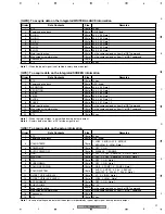
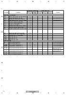
Page 102: ... main unit and remote controller O FCLS04 Setting the memory lock O OSD DOF Erasing the currently OSD displyed indications O O DISPLAY CALL DITS01 Displaying the DISPLAY CALL 1 O O DITS02 Displaying the DISPLAY CALL 2 O O IM0 Writing the INFORMATION 1 3 characters O O IM1 Writing the INFORMATION 4 6 characters O O IM2 Writing the INFORMATION 7 9 characters O O IM3 Writing the INFORMATION 10 12 cha...

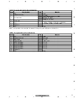
Page 103: ...Setting the color difference selection to RGB VIDEO O O MCDS02 Setting the color difference selection to COMPONENT1 Y CbCr O O MCDS03 Setting the color difference selection to COMPONENT2 Y PbPr O O COLOR SYSTEM CLSS01 Setting the color system to AUTO O CLSS02 Setting the color system to NTSC O CLSS03 Setting the color system to PAL O CLSS04 Setting the color system to SECAM O CLSS05 Setting the co...

Page 104: ...er time ON O TPH Setting the time of current time O O O 000 023 TPM Setting the minute of current time O O O 000 059 TPW Setting the day of current time O O O 001 007 TPTS00 Turning the program timer OFF O TPTS01 Turning the program timer ON O ORBITER ORBS00 Turning the orbiter OFF O ORBS01 Turning the orbiter ON AUTO1 O ORBS02 Turning the orbiter ON AUTO2 O ORBS03 Turning the orbiter ON AUTO3 O S...

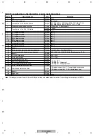
Page 105: ...ting the color detail blue O O 000 060 CGM Adjusting the color detail magenta O O 000 060 GAMMA GRAS18 Setting the gradation to GAMMA 1 8 O GRAS19 Setting the gradation to GAMMA 1 9 O GRAS20 Setting the gradation to GAMMA 2 0 O GRAS21 Setting the gradation to GAMMA 2 1 O GRAS22 Setting the gradation to GAMMA 2 2 O GRAS23 Setting the gradation to GAMMA 2 3 O GRAS24 Setting the gradation to GAMMA 2 ...

Page 106: ...25 O MGPSnn nn 01 04 DIVIDER Set display position of 4 00 there is no joint consideration O nn 05 08 DIVIDER Set display position of 4 00 there is joint consideration O nn 10 18 DIVIDER Set display position of 9 00 there is no joint consideration O nn 20 28 DIVIDER Set display position of 9 00 there is joint consideration O nn 30 3F DIVIDER Set display position of 16 00 there is no joint considera...

Page 107: ...Setting the IMAGE PROCESS to PURE O IPRS03 Setting the IMAGE PROCESS to MONOTONE O IPRS04 Setting the IMAGE PROCESS to HIGH CONTRAST O FRC FRCS00 Turning the FRC OFF O FRCS01 Turning the FRC ON O SEAMLESS INPUT SWITCH SLSS00 Turning the SEAMLESS input switch mode OFF O SLSS01 Turning the SEAMLESS input switch mode ON O SL1S01 Setting the SEAMLESS SW SELECT 1 to INPUT1 O SL1S02 Setting the SEAMLESS...

Page 108: ...ing the BANNER PinP input to INPUT2 O BPPS00 Setting the BANNER PinP to OFF O BPPS01 Setting the BANNER PinP to TOP O BPPS02 Setting the BANNER PinP to MID HIGH O BPPS03 Setting the BANNER PinP to MID LOW O BPPS04 Setting the BANNER PinP to BOTTOM O FUNCTION DEFAULT FDT Executing the FUNCTION DEFAULT O Other command Command Operation Command Effectiveness Numeric Direct input Remarks Factory Norma...

Page 109: ...5 MBG Adjusting the B GAIN of AD MAIN O O 000 255 MBO Adjusting the B OFFSET of AD MAIN O O 000 255 SRG Adjusting the R GAIN of AD SUB O O 000 255 SRO Adjusting the R OFFSET of AD SUB O O 000 255 SGG Adjusting the G GAIN of AD SUB O O 000 255 SGO Adjusting the G OFFSET of AD SUB O O 000 255 SBG Adjusting the B GAIN of AD SUB O O 000 255 SBO Adjusting the B OFFSET of AD SUB O O 000 255 Various cont...

Page 110: ...panel drive mode to TYPE A VD movie2 O O PAVS06 Setting the panel drive mode to TYPE A VD viewer O O PAVS07 Setting the panel drive mode to TYPE A VD USER O O PAVS08 Setting the panel drive mode to TYPE A VD ISFDAY O O PAVS09 Setting the panel drive mode to TYPE A VD ISFNGT O O PAVS10 Setting the panel drive mode to TYPE B VD factory O O PAVS11 Setting the panel drive mode to TYPE B VD STD O O PAV...

Page 111: ...tents as item 13 of QS2 comman 2Byte 18 Sixth latest PD infromation 1st 1Byte As the same contents as item 6 7 of QS2 comman 19 Sixth latest PD infromation 2nd 1Byte 20 HOUR METER for the sixth latest PD 6Byte As the same contents as item 13 of QS2 comman 2Byte 21 Seventh latest PD infromation 1st 1Byte As the same contents as item 6 7 of QS2 comman 22 Seventh latest PD infromation 2nd 1Byte 23 HO...

Page 112: ...ff O O MKSS01 Pattern mask PATTERN01 set to H RAMP lean 1 O MKSS02 Pattern mask PATTERN02 set to H RAMP lean 4 O MKSS03 Pattern mask PATTERN03 set to V RAMP lean 1 O MKSS04 Pattern mask PATTERN04 set to slant RAMP O MKSS05 Pattern mask PATTERN05 Window Hi 870 Lo 102 O MKSS06 Pattern mask PATTERN06 Window Hi 1023 Lo 102 O MKSS07 Pattern mask PATTERN07 Window Hi 1023 O MKSS08 Pattern mask PATTERN08 ...

Page 113: ...o sky blueX2 O MKSS71 Raster mask RASTER21 set to light purple X O MKSS72 Raster mask RASTER22 set to blue 960 O MKSS73 Raster mask RASTER23 set to yellow 512 O MKSS74 Raster mask RASTER24 set to gray 512 O AM radio noise counterplan SFRS01 Setting AM radio noise counterplan to pattern 1 O SFRS02 Setting AM radio noise counterplan to pattern 2 O SFRS03 Setting AM radio noise counterplan to pattern...

Page 114: ...ata to digital Assy O UAJ Returning the digital ASSY to service parts O FAJ Determining the main unit adjustment O SHIS01 Setting the SHIP to S J O SHIS02 Setting the SHIP to G O SHIS03 Setting the SHIP to CKD O Various protection IJN Turning the alarm detection off O Do not perform the main SHUT DOWN detection IJY Turning the alarm detection on O Perform the main SHUT DOWN detection SDMS00 Turnin...

Page 115: ...n input a numeric command value that has been converted from the voltage value using the 2 or 3 key Clearance of various logs for the panel such as that for the hour meter value It is required to clear various data such as the data on the hour meter value etc to match the drive time of the panel Write down the hour meter value at the time of the replacement in the margin of the label shown above T...

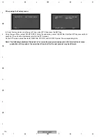
Page 116: ...ressed for 5 seconds The unit will automatically return to the ETC screen On the ETC screen select the items PM B1 B5 PD INFO and SD INFO to clear the corresponding data Note The following adjustment flowchart is for currently mass produced panels After termination of mass production of the product the adjustment flowchart for the next product may be different PANEL FACT VD1 11601 NTV 4MX ETC TBL4...

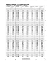
Page 117: ...OF062 25 67 VOF107 34 08 VOF152 42 48 VOF018 17 45 VOF063 25 86 VOF108 34 26 VOF153 42 67 VOF019 17 64 VOF064 26 04 VOF109 34 45 VOF154 42 86 VOF020 17 83 VOF065 26 23 VOF110 34 64 VOF155 43 04 VOF021 18 01 VOF066 26 42 VOF111 34 82 VOF156 43 23 VOF022 18 20 VOF067 26 61 VOF112 35 01 VOF157 43 42 VOF023 18 39 VOF068 26 79 VOF113 35 20 VOF158 43 60 VOF024 18 57 VOF069 26 98 VOF114 35 38 VOF159 43 7...

Page 118: ... VOF243 59 48 VOF199 51 26 VOF244 59 67 VOF200 51 45 VOF245 59 86 VOF201 51 64 VOF246 60 04 VOF202 51 82 VOF247 60 23 VOF203 52 01 VOF248 60 42 VOF204 52 20 VOF249 60 60 VOF205 52 38 VOF250 60 79 VOF206 52 57 VOF251 60 98 VOF207 52 76 VOF252 61 16 VOF208 52 94 VOF253 61 35 VOF209 53 13 VOF254 61 54 VOF210 53 32 VOF255 61 72 VOF211 53 50 VOF212 53 69 VOF213 53 88 VOF214 54 06 VOF215 54 25 VOF216 54...

Page 119: ...5 VRP023 246 3 VRP068 265 8 VRP113 285 4 VRP158 304 9 VRP024 246 7 VRP069 266 2 VRP114 285 8 VRP159 305 3 VRP025 247 1 VRP070 266 7 VRP115 286 2 VRP160 305 8 VRP026 247 6 VRP071 267 1 VRP116 286 7 VRP161 306 2 VRP027 248 0 VRP072 267 5 VRP117 287 1 VRP162 306 6 VRP028 248 4 VRP073 268 0 VRP118 287 5 VRP163 307 1 VRP029 248 9 VRP074 268 4 VRP119 288 0 VRP164 307 5 VRP030 249 3 VRP075 268 9 VRP120 2...

Page 120: ...2 3 VRP243 341 8 VRP199 322 7 VRP244 342 3 VRP200 323 2 VRP245 342 7 VRP201 323 6 VRP246 343 1 VRP202 324 0 VRP247 343 6 VRP203 324 5 VRP248 344 0 VRP204 324 9 VRP249 344 4 VRP205 325 3 VRP250 344 9 VRP206 325 8 VRP251 345 3 VRP207 326 2 VRP252 345 7 VRP208 326 6 VRP253 346 2 VRP209 327 1 VRP254 346 6 VRP210 327 5 VRP255 347 0 VRP211 327 9 VRP212 328 4 VRP213 328 8 VRP214 329 2 VRP215 329 7 VRP216...

Page 121: ...NB Assy MD DIGITAL Assy SUS CLAMP 2 Assy SEND Assy SUS CLAMP 1 Assy LED2 Assy KEY Assy COMMSLOT IF Assy VSIF Assy AUDIO Assy SENC Assy COMMSLOT Assy 42 SCAN B Assy 42 Y DRIVE Assy MAIN Assy 42 X DRIVE Assy POWER SUPPLY Unit 42 SCAN A Assy 42 ADDRESS Assy 42 ADDRESS Assy 42 ADDRESS Assy 42 ADDRESS Assy ...

Page 122: ...0 ms for 1 to n times 1 in one burst with 2500 ms of pause between switching Green flashes at inter vals of 500 ms for 1 to n times 2 in one burst with 2500 ms of pause between switching Red lit and green flashes at intervals of 200 ms Power management Power down Shutdown 1 For the frequency of flashing during power down see the PD sheet 2 For the frequency of flashing during shut down see the SD ...

Page 123: ... generated power down data are referred to If power downs are found in both the 1st and 2nd set of PD data the 1st set of PD data is referred to and the 2nd set of PD data is ignored PD information 3 SCAN PD information 4 SCN 5V PD information 5 Y DRV PD information 6 Y DCDC PD information 7 Y SUS PD information 8 ADRS PD information 9 X DRV PD information A X DCDC PD information B X SUS PD inform...

Page 124: ...or SUSOUT and SUSGND 4 SCN 5V SCAN A B CN2401 CN2402 IC5V UVP SCAN IC SCAN IC Y DRIVE IC5V DC DC Q2605 R2647 Y SUS BLOCK R2352 6 Y DCDC Y DRIVE VOFS UVP VOFS DC DC Q2606 R2619 R2620 Y SUS BLOCK IC2252 IC2253 Q2280 Q2281 Short circuiting between MSKS and SUSOUT Vprst UVP Vprst Regulator Q2531 Q2532 IC2535 7 Y SUS Y DRIVE Detection of midpoint voltage PD Y RESONANCE BLOCK IC2101 Y SUS BLOCK Q2221 8 ...

Page 125: ...DOWN1 detection VCC DOWN2 detection LED Display Pattern Remarks Color Flashing Frequency Green Green Green Green Green Green Green Green Green Green Green Green Green Green 1 2 3 4 5 6 8 9 10 11 12 13 14 15 Repeat Repeat Repeat Repeat Repeat Repeat Repeat Repeat Repeat Repeat Repeat Repeat Repeat Repeat 1 1 Triggered by an REQ_MD signal a QS2 command is issued to acquire data on the status of the ...

Page 126: ...AUDIO Defective AMP IC IC3002 AUDIO Defective AUDIO CONTROL IC IC3001 MAIN Defective buffer IC5306 AUDIO Disconnection of connector CN9001 CN3004 Check if the connector is disconnected or not securely connected 6 Communication failure in module microcomputer DIGITAL Communication failure of the module microcomputer or defective peripheral circuits MODULE UCOM BLOCK IC3151 Check if the communicatio...

Page 127: ... ASSY TXD VS RXD VS VIDEO SLOT I F ASSY CN4006 IC5306 Audio Buffer IC6301 IC6 VIDEO SIGNAL OE IC9508 EEPROM IC5304 Expand I O POWER SUPPLY UNIT AUDIO ASSY MAIN ASSY 0 0 8 6 1 2 2 2 3 4 8 8 8 8 8 8 5 PN1 CN9003 CN9004 CN9501 SENC ASSY IC1101 SEND ASSY IC1201 SENB ASSY IC1001 CN1001 CN1101 CN1201 CN5301 CN4004 DIGITAL ASSY IC3401 Sequence Processor ASTRA IC3304 1 2V Reset IC3302 3 3V Reset IC3157 DA...

Page 128: ... a failure in the MAIN PWB In a case of an audio related abnormality such as no sound Proceed to 3 Abnormality in audio P148 In a case when a remote control unit does not function Proceed to 4 Failure of a remote control unit P152 Note If symptoms persist after replacement of parts such as ICs following the diagnosis results of this failure analysis chart it is recommended to replace the whole PC ...

Page 129: ...PDP 425CMX 129 5 6 7 8 5 6 7 8 C D F A B E ...

Page 130: ...IC5308 IC5603 IC5002 IC5001 IC5904 IC9504 IC5603 IC5604 IC700 CN9001 IC5004 CN5001 IC5605 CN4005 IC5605 IC5604 CN5301 4 6 7 8 11 3 3 32 5 9 1 2 13 CN9502 T13 IC9503 T14 CN530 T14 IC7006 T20 T CN901 T13 CN901 T41 IC5308 T34 45 11 42 46 21 22 24 24 12 18 16 IC5004 T60 IC700 T20 IC5604 T51 IC5603 T51 IC5904 T56 IC5005 T60 SIDE A ...

Page 131: ...9012 CN9011 CN8502 IC8003 CN6301 IC8002 IC700 IC5904 IC9504 IC5604 IC4003 IC7001 CN4001 IC8501 8 11 28 29 3 5 33 9 1 IC7006 T20 PM T12 PM2 T22 PM1 T22 CN9011 T14 IC8002 T22 IC8003 T22 CN8502 T14 16 29 00 20 IC5604 T51 IC8501 T22 IC4003 T54 CN400 T54 IC5904 T56 SIDE A ...

Page 132: ...PDP 425CMX 132 1 2 3 4 1 2 3 4 C D F A B E MAIN PWB CONNECTOR WAVE FORM POINT SIDE B ...

Page 133: ...PDP 425CMX 133 5 6 7 8 5 6 7 8 C D F A B E X5008 X5008 34 35 IC6304 IC6302 29 29 IC6302 29 SIDE B ...

Page 134: ...PDP 425CMX 134 1 2 3 4 1 2 3 4 C D F A B E SUB PWB 43 44 CN240 T41 IC3002 IC3001 IC3002 T31 L3006 T31 L3005 T31 CN2401 CONNECTOR WAVE FORM POINT SIDE A ...

Page 135: ...PDP 425CMX 135 5 6 7 8 5 6 7 8 C D F A B E 44 45 IC3001 CN2301 CN2303 IC2301 CN3004 IC2301 T41 CN230 T13 CN230 T13 SIDE A ...

Page 136: ...Analog Audio signal IC7003 5V to 3 3V IC5605 Sync sep 5V IC5903 Sync sep 5V IC5604 SW IC5602 LPF 5V 5V IC5905 LPF IC5904 SW 3 3V IC5606 BUF 5V CN5002 INPUT1 IC5001 BUF IC5002 IC6301 OE IC5004 Video SW CN5003 IC5007 BUF 3 3V 3 3V 9V IC5005 SyncSW IC5008 BUF LPF LPF VIDEO SLOT IC2201 X2201 3 84MHz VIDEO SLOT I F ASSY CN4006 CN4001 CN4002 CN4003 CN4004 CN4005 CN6301 CN6302 CN5301 COMM SLOT ASSY COMM ...

Page 137: ...01 CN8502 FAN 3 H G To Md 2 2 CN9010 CN9501 IC8105 OSD 3 3V IC8501 LVDS Transmitter 3 3V L R IC8101 8104 SDRAM 3 3V IC9502 7V to 5V 7V IC6501 A D Converter 3 3V X9501 33 333MHz IC6701 A D Converter 3 3V 3 3V IC8001 Digital signal Processor 3 3V IC9504 BUF 3 3V 11 19 31 32 36 38 41 43 47 48 2 27 9V AUDIO ASSY 9V IC3002 Audio Amplifier CN3004 CN3003 CN3001 IC3004 12V to 9V 12V IC3001 Audio Controlle...

Page 138: ...tor lit YES NO When POWER SATNDBY indicator turns on red perform the power on operation with the remote control unit or the RS232C command See Other causes for shutdown of Failure Diagnosis by LEDs Note When an abnormality is detected and indicated by LEDs flashing or lighting all power supply lines except for the 7 V DC M 7 V and 5 V DC M 5 V lines will be automatically shut off after about 10 se...

Page 139: ...output from Pin 14 of CN8502 AD2 YES Failure in the MAIN PWB failure in IC9501 or X9501 Note If IC9501 is in failure replace the whole board Failure in the AD2 connector or MAIN PWB failure in IC9501 or X9501 Note If IC9501 is in failure replace the whole board A Turn the main power on with the cable to the CN2401 or CN2301 disconnected Check if 5 V DC is output from Pin 8 of CN2301 Turn the main ...

Page 140: ...onnector or the PDP To Examination of the MAIN board Failure in the PDP YES Is reset discharge seen lighting When SD or PD information is acquired using the QS2 command of RS 232C is any abnormality detected Turn the power off at the Main Power Switch then back on 2 Abnormality in images ...

Page 141: ...3 0 V and 0 V DC NO YES YES YES NO NO NO NO YES YES Are signals input to Pins 2 30 and 31 for control of IC5301 Are signals input to Pins 4 and 7 of IC5604 Is the voltage at Pin 1 of IC5604 0 V DC NO NO NO YES Failure in the MAIN PWB Failure in the MAIN PWB NO NO YES YES YES YES Are signals input to Pins 2 30 and 31 for control of IC5301 Are signals input to Pins 11 and 13 of IC5605 Are signals in...

Page 142: ...e in the IC4003 Are 13 5V supplied to pin 3 of IC4003 Are 3 3V supplied to pins 7 and 8 of CN4001 Are 3 3V supplied to pin 11 of CN4001 When either input from SLOT does not come out Examination of the SLOT Examination of the SLOT power supply Failure in the POWER unit or harness ADX3275 Failure in the POWER unit or harness ADX3275 Failure in the POWER unit or harness ADX3275 Failure in the POWER u...

Page 143: ...rom VIDEO SLOT PWB NO NO NO NO YES Failure in the I F PWB or flexible cable Are the sync and clock signals input to pins 1 2 and 4 of CN6301 YES Failure in the IC6302 and peripheral parts Failure in the IC6301 and peripheral parts Failure in the IC6304 and peripheral parts Is the clock signal input to pin 2 of IC6302 YES Are the sync and clock signals input to pins 168 169 and 172 of IC6301 YES Is...

Page 144: ...5902 Are signals input to Pins 2 4 and 30 for control and Pin 31 3 3V DC of IC5301 NO YES NO YES YES NO Are signals input to Pins 11 and 13 of IC5903 Failure in the IC9504 Failure in the IC5903 Failure in the IC5301 Failure in the IC5301 Failure in the IC5001 Failure in the IC5904 Failure in the IC5902 NO Are signals input to Pins 3 and 6 of IC9504 YES YES YES Are signals input to Pins 7 and 9 for...

Page 145: ...input to Pins 15 13 and 10 for video of IC5007 Is the voltage at Pin 16 of IC5004 5V DC Check the signal output equipment and its cables Check the signal output equipment and its cables NO Verification of the sync section Examination of the MAIN board Check the connected equipment and its cables NO Failure in the IC5604 Are signals input to Pins 2 30 and 31 for control of IC5301 Failure in the IC5...

Page 146: ...ilure in the IC5605 Failure in the IC5606 Failure in the MAIN PWB Failure in the MAIN PWB Failure in the MAIN PWB YES NO Is the voltage at Pin 1 of IC7006 7 V DC Check the signal output equipment and its cables YES NO Are sync signals input to Pins 48 and 47 of IC7001 And is a CLK signal input to Pin 44 of IC7001 NO Are sync signals input to Pins 7 and 9 of IC5603 YES NO Are sync signals input to ...

Page 147: ...N2 connector Check if 2 5V DC is output from Pin 1 of PN2 Failure in the power supply unit or PN2 cable broken NO NO NO NO Is the voltage at Pin 1 of PN2 connector 2 5 V DC YES Is the voltage at Pin 4 of IC8002 1 5 V DC Failure in the MAIN PWB Failure in the MAIN PWB Failure in the MAIN PWB YES NO YES Is the voltage at Pin 5 of IC8003 1 5 V DC NO YES Is a CLK signal input to Pin 3 of X8001 Is a CL...

Page 148: ... IF board PCB connectors or video slot card If the audio signal is output after the video slot card is replaced by a normally operating one the removed video slot card was defective YES Failure in the AUDIO PWB Failure in the IC3002 Failure in the IC5308 YES NO Does the green POWER indicator repeat a burst of 5 flashes even after the CN3004 AU connector cable is disconnected YES Is the voltage at ...

Page 149: ... connector CN3003 on the AUDIO PWB YES Is the audio signal waveform output from Pin 11 of IC3001 Are the waveforms shown below output from the AU connector CN3004 on the MAIN PWB NO Pin_No 1 2 3 4 5 6 Name S 12 S 12 S 12 GND GND GND Voltage 12 5Vdc 12 5Vdc 12 5Vdc GND GND GND Pin 8 Pin 9 Pin 7 Pin 5 Pin 8 Pin 9 Pin 7 Pin 5 Pins 1 and 3 Audio signal waveform 5Vpp 5Vpp 9 0Vdc 3 3Vdc Failure in the C...

Page 150: ...pment Note When INPUT 2 input is selected you can observe waveform at IC5308 3pin NO YES Is the audio signal waveform input to Pin 15 of IC5308 Failure in the IC5306 Failure in the IC5308 NO NO YES When INPUT1 input is selected is the audio signal waveform input to Pin 1 of IC5308 B Waveform 46 Waveform 46 ...

Page 151: ... No sound when the connected equipment is terminated with 75 ohms YES NO Is 12 Vdc power input to Pin 14 of IC5308 Failure in IC5308 or IC5306 YES NO Is an audio waveform output from the audio input terminal of IC5308 Pin 1 for INPUT 1 Pin 3 for INPUT 2 or Pin 5 for video slot input Failure in the equipment connected via the input connector or poor connection of the audio input connector YES NO Is...

Page 152: ...low output from Pin 6 of CN9010 on the MAIN PWB NO 5Vp p YES Is the signal shown below output from Pin 1 of CN2401 on the LED PWB NO 4 4Vp p Failure in the IC2301 of COMM SLOT I F PWB Failure in the Q2302 or Q2301 of COMM SLOT I F PWB YES Is the signal shown below output from Pin 10 of IC2301 on the COMM SLOT I F PWB NO 4Vp p 1V 4 Failure of a remote control unit ...

Page 153: ...PDP 425CMX 153 5 6 7 8 5 6 7 8 C D F A B E Waveform 8 Waveform 4 Waveform 1 2 Waveform 9 Waveform 5 Waveform 2 Waveform 10 1 Waveform 6 Waveform 3 Waveform 10 2 Waveform 7 Waveform 1 1 ...

Page 154: ...PDP 425CMX 154 1 2 3 4 1 2 3 4 C D F A B E Waveform 11 1 Waveform 17 Waveform 13 Waveform 11 2 Waveform 18 Waveform 14 Waveform 12 1 Waveform 19 Waveform 15 Waveform 12 2 Waveform 20 1 Waveform 16 ...

Page 155: ...PDP 425CMX 155 5 6 7 8 5 6 7 8 C D F A B E Waveform 20 2 Waveform 29 1 Waveform 24 Waveform 21 Waveform 29 2 Waveform 25 Waveform 22 Waveform 30 Waveform 26 Waveform 23 Waveform 31 Waveform 28 ...

Page 156: ... 44 Waveform 35 Waveform 33 1 Waveform 45 Waveform 41 Waveform 33 2 Waveform 46 Waveform 42 Waveform 34 Waveform 43 Conditions of signal input Audio input connector AUDIO 1 or Video slot card L ch Input signal level 200mVrms Input signal frequency 1 kHz Volume Max ...

Page 157: ...stems during a repair etc 2 In a case where diagnosis is required for judging whether the power to the large power signal system or small signal system has been down when a power down occurred Methods Switch off the large power signal system swtich S3601 downward on the MD DIGITAL Assy Notes When the power to the large power signal system is off as the PD signal is muted power downs other than PS_...

Page 158: ... Do NOT send backup data 2 Replacement of IC3161 IC3161 is the EEPROM for backup When IC3161 is to be mounted on the MD DIGITAL Assy for service transmission of backup data is required See How to back up adjustment data for the main unit next page How to replace the EEPROM Data such as adjustment data for the module are stored in the EEPROM on the MD DIGITAL Assy When the MD DIGITAL Assy is to be ...

Page 159: ...ata Adjustment value of the upper limit of the power supply Pulse meter data Panel WB adjustment value Serial number Drive waveform adjustment value P ON Power on counter data PD SD Power down shutdown log data How to copy backed up data Method 1 After the original backup EEPROM is mounted on the MD DIGITAL Assy for service copy the backup data by either Method 1 or 2 Using RS 232C commands FAY BC...

Page 160: ...or 3 seconds Press the keys in the following order LEFT UP LEFT RIGHT then POWER PANEL INFORMATION ETC down down down down MENU ENTER BACKUP DATA DIGITAL EEPROM Item Content Services RS 232C Command Panel replacement Power unit replacement Other than those at left Hour meter Accumulated display time Clearing required Clearing not required Clearing not required CHM Shutdown logs Location where an S...

Page 161: ...essed for 5 seconds right To clear SD logs HR MTR INFO NO HR MTR INFO CLEAR down MENU ENTER Hold the keys pressed for 5 seconds right To clear hour meter data PM B1 B5 INFO NO PM B1 B5 INFO CLEAR down MENU ENTER Hold the keys pressed for 5 seconds right To clear pulse meter data P COUNT INFO NO P COUNT INFO CLEAR down MENU ENTER Hold the keys pressed for 5 seconds right To clear power on count dat...

Page 162: ...then back on Fixed at H Vertically or inversely situated OSD ANGLE V or MIRROR MODE Y or XY Fixed at H Vertically or inversely situated FAN Rotation Speed Without Slot or With a Slot Made by Pioneer With a Slot Made by Another Manufacturer OFF L 68 55 L M 70 65 M H 74 69 Abnormal temperature 82 82 Unit ºC The rotation speed of the fan is switched as shown in Table 1 above upon detecting the temper...

Page 163: ...microcomputer to boot it 5 The MD microcomputer issues the REQ_MD signal to the main microcomputer QS2 data read request 6 After confirming the QS2 data read request confirming SD or PD the main microcomputer issues PON 7 The MD microcomputer sends a PON echo back to the main microcomputer 8 The MD microcomputer issues the RELAY signal to turn on the unit REMI M 3 3V KEY ASSY MAIN ASSY Front key L...

Page 164: ...MX Assy COMM bracket CMX POWER SUPPLY Multi base CMX SUS CLAMP 1 SUS CLAMP 2 MAIN VSIF AUDIO SENB SENC SEND KEY LED2 COMMSLOT COMMSLOT IF SCAN IC 42 X DRIVE MD DIGITAL 42 Y DRIVE Fan motor 80 25L Note 1 Even if the unit shown in the photos and illustrations in this manual may differ from your product the procedures described here are common Note 2 For performing the diagnosis shown below the follo...

Page 165: ...ront Case Assy 425CMX 1 1 Remove the four screws AMZ30P060FTB 2 Pull the lower part of the Front case Assy 425CMX toward you and out 3 Remove the Front case Assy 425CMX by pulling it upward Front case Assy 425CMX Front case Assy 425CMX Rear case 1 2 3 1 1 1 ...

Page 166: ... screws AMZ30P060FTB 2 Remove the bottom cover CMX 2 2 2 2 2 2 2 2 2 2 2 2 2 2 1 1 1 1 3 1 1 1 1 1 1 1 2 1 1 1 1 1 1 1 1 Rear case Bottom cover CMX 1 Two screws AMZ30P060FTB 1 2 About reattachment For easy reattachment be sure to install the screws for the Rear case in the order indicated in the photo After securing those screws in place the other screws can be reattached in any order ...

Page 167: ...Disconnect cables as required 3 Remove the COMM bracket Block COMM bracket Block AC bracket Block COMM Bracket Block 1 Remove the two screws 2 Remove the one screw 3 Disconnect cables as required 4 Remove the AC bracket Block AC Bracket Block 1 1 1 1 1 2 COMMSLOT Assy AUDIO Assy SENC Assy COMMSLOT IF Assy 3 4 ...

Page 168: ...3 4 1 2 3 4 C D F A B E Multi Base Block 5 1 Remove the two screws 2 Remove the one screw 3 Remove the one screw 4 Disconnect cables as required 5 Remove the multi base Block Multi base Block 1 1 3 2 5 VSIF Assy MAIN Assy ...

Page 169: ...ar case See step ø 3 Remove the bottom cover See step π 4 Remove the three screws 5 Remove the COMM bracket section 6 Remove the three screws 7 Remove the four screws 8 Remove the front chassis LB 6 6 6 7 7 7 7 Front chassis LB 42 SCAN B Asssy SCAN IC 6 42 SCAN A Asssy 4 4 4 COMM bracket section 5 8 SCAN IC 6 Exchange ...

Page 170: ...0 73 OUT59 72 OUT58 71 OUT57 70 OUT56 69 OUT55 68 OUT54 67 OUT53 66 OUT52 65 OUT51 64 OUT50 63 OUT49 62 OUT48 61 OUT47 60 OUT46 59 OUT45 58 OUT44 57 OUT43 56 OUT42 55 OUT41 54 OUT40 53 OUT39 52 OUT38 51 OUT2 100 OUT1 99 N C 98 V DDH 97 V DDH 96 N C 95 GND1 94 GND1 93 CLR 92 SI 91 OC2 90 OC1 89 V DD 88 LAT 87 CLK 86 SO 85 DIR 84 GND1 83 GND1 82 N C 81 V DDH 80 V DDH 79 N C 78 OUT64 77 OUT63 76 26 O...

Page 171: ...ply 81 N C Not connected 82 83 GND1 Ground 84 DIR I Setup of shift register shift direction L Shift into reverse SO SI H Shift forward SI SO 85 SO I O Serial data input output 86 CLK I Serial clock input Fetch SI or SO data to shift register by CLK rise edge 87 LAT I LAT data input L Transfer shift register data to output latch H Hold data to output latch 88 VDD Logic supply 89 OC1 I Output contro...

Page 172: ...rangement Top view Block Diagram Truth Table IN B A B Y L L L L H L H L L H H H 1 IN A 2 GND VCC OUT Y 3 5 4 TC74VHC00FTS1 42 X DRIVE ASSY IC1002 Quad 2 Input NAND Gate Block Diagram Truth Table 1A 1 Vcc 14 1B 2 4B 13 1Y 3 4A 12 2A 4 4Y 11 2B 5 3B 10 2Y 6 3A 9 GND 7 3Y 8 A B Y L L H L H H H L H H H L ...

Page 173: ...0 5V 21 15V 22 Delay Circuit Driver 43 PSUS 42 PSUS 41 PSUS 40 PSUS 39 PSUS 38 PSUS 33 PSUS 32 PSUS 31 PSUS 30 PSUS 29 PSUS 28 PSUS 27 SUBGND 23 SUS MSK 26 AXF1145 42 X DRIVE ASSY IC1101 42 Y DRIVE ASSY IC2101 DK Module Block Diagram PC PL D 3 PL U 10 SUSOUT 15 SUSOUT 16 SUSOUT 17 SUSOUT 18 PL U 11 PL U 12 PL U 13 PD U 8 PC 4 PC 5 PC 6 41 PL D 40 PL D 39 PL D 38 CO D 36 CI D Driver Delay Circuit 1...

Page 174: ... 10 3B 9 3A 8 3Y A B Y L L L L H L H L L H H H AXF1144 42 Y DRIVE ASSY IC2252 IC2253 Y Mask Module Block Diagram SUSOUT 1 SUSOUT 2 SUSOUT 3 SUSOUT 4 SUSGND 7 SUSGND 6 SUSGND 8 SUSGND 9 SUSGND 10 VSUS 13 VSUS 12 VSUS 14 VSUS 15 VSUS GND 18 SUS G 19 SUS B 20 5V 21 15V 22 Delay Circuit Driver PSUS 33 PSUS 32 PSUS 31 PSUS 37 PSUS 38 PSUS 39 PSUS 40 PSUS 36 PSUS 30 PSUS 29 SUBGND 23 MSK S 27 MSK S 26 M...

Page 175: ... Diagram Pin Function AO1 1 AO2 2 AO3 3 AO4 GND SDA SCL VCC 4 8 7 6 5 1A 1 Vcc 16 1B 2 1Rx Cx 15 1CLR 3 1Cx 14 1Q 4 1Q 13 2Q 5 2Q 12 2Cx 6 2CLR 11 2Rx Cx 7 2B 10 GND 8 2A 9 8 8bit Latch 8bit Upper Segment R 2R 2 8bit Latch 8bit Upper Segment R 2R 3 7 6 8bit Latch 8bit Upper Segment R 2R 4 5 No Pin Name Pin Function 1 AO1 8 bit resolution D A converter output 2 AO2 3 AO3 4 AO4 5 GND Ground 6 SDA Se...

Page 176: ...nt Electrostatic protection element 2 PST3610UR MD DIGITAL ASSY IC3304 Reset IC Pin Arrangement Top view Block Diagram Pin Function GND 1 VDD CD OUT 2 4 3 1 4 3 No Pin Name Pin Function 1 GND Ground 2 VDD Power supply Voltage detection 3 CD Capacitor connect pin for delay 4 OUT Reset signal output ...

Page 177: ...N1 CSCS_N2 CSIOSCK1 CSIORXD EXA15 EXA19 CSCS_N0 GND33 TCRAM_MONITOR0 TCRAM_MONITOR1 EXA14 EXA18 UARTRXD VDD33 TCRAM_MONITOR2 CSIORQ EXA13 EXA17 UARTTXD CS10TXD RESETX SDIJTAG EXA12 CSEXWAIT_N SDITRST_N SDITCK SDIDBI_N SDITMS GND12 SDITDO SDITDI GPI000 GPI001 GPI002 CSRD_N CLKS VSSPB VCCPB LPFMONI VCCPA CLK_MONI EXDI014 EXDI07 EXDI015 EXDI04 EXDI012 EXDI05 EXDI013 EXDI06 GND33 VDD33 EXDI02 EXDI010 ...

Page 178: ...PDP 425CMX 178 1 2 3 4 1 2 3 4 C D F A B E Pin Layout Block Diagram DS90CF388VJD MD DIGITAL ASSY IC3001 LVDS Receiver ...

Page 179: ...tes 1 DESKEW I 4 Deskew and oversampling on off select Deskew is active when in put is high Only supported in DC Balance mode BAL High To complete the deskew operation a minimum of four clock cycles is required during blanking time PD I 78 TTL level in put When asserted low input the receiver data outputs are low and clock out put is high STOPCLK O 73 Indicates receiver clock in put signal is not ...

Page 180: ...ndby mode The indicator lights red When flashing the indicator is used to indicate error messages 5 Handles Operation panel on the main unit 6 STANDBY ON button Press to put the display in operation or standby mode 7 MENU button Press to open and close the on screen menu 8 DISPLA Y SET button Use to confirm onscreen menu selections and to change settings When not indicated by onscreen menus used t...

Page 181: ...l will not be output from the ANALOG RGB OUT INPUT1 terminal when the main power of this unit is off or in standby mode 7 ANALOG RGB IN INPUT1 mini D sub 15 pin For connection of a personal computer PC or similar component Make sure that the connection made corresponds to the format of the signal output from the connected component 8 DIGITAL RGB INPUT2 DVI D jack Use to connect a computer Note Thi...

Page 182: ...essional installers 0 AUTO SET UP button When using computer signal input automatically sets the POSITION CLOCK and PHASE to optimum values STANDBY ON button Press to put the unit in operation or standby mode DISPLA Y button Press to view the unit s current input and setup mode POINT ZOOM button Use to select and enlarge one part of the screen FREEZE button When memo screen function is enabled a s...

Page 183: ... T M D S Data1 3 Shield NC No connection NC No connection 5V Power GND Hot Plug Detect T M D S Data0 T M D S Data0 T M D S Data0 5 Shield NC No connection NC No connection T M D S Clock Shield T M D S Clock T M D S Clock Pin No 5 1 15 11 6 10 INPUT1 2 pin assignments INPUT1 Mini D sub 15 pin female connector pin allocation Input Output 1 2 3 4 5 6 7 8 9 10 11 12 13 14 15 R G B NC No connection GND...

Page 184: ...t be sure to clean the following positions by using the prescribed cleaning tools Position to be cleaned Cleaning tools Fans Cleaning paper GED 008 Jigs list GGD1469 Extension cable for 42inch PDP diagnosis GGP1075 Extension cable for 42inch PDP diagnosis Jig No Name Remarks ...

Reviews: