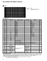
background image

82

PDP-503CMX, PDP-503MXE, PDA-5002

O F S

C O N

R

T

A S T

(

)

– R G B 2

S 1

I N 4 – 0 2 –

*

* * *

* * *

2

N T

# 1

1

1

5

10

15

16

5

10

15

20

25

30

35

40

Rem Code

Key Name

Function & Display

Description

Remarks

Lower 

Layer

AA01

1

CONTRAST

Call the 

adjustment value 

and display it.

×

AA02

2

BRIGHT

×

AA03

3

COLOR

×

AA04

4

TINT

R HIGH

G HIGH

B HIGH

R LOW

G LOW

B LOW

×
×
×
×
×
×
×

AA05

5

AA06

6

AA07

7

AA08

8

AA09

9

AA00

10

AA46

11

AA47

12

AA4D

BS1

AA4E

BS3

AA4F

BS5

AA50

BS7

AA51

BS9

AA52

BS11

AA53

BS13

AA54

BS15

AA96

5

Select upper item

AA97

Select lower item

Adjustment value of the parameter selecting goes up.

Adjustment value of the parameter selecting goes down.

Store the adjustment value and shift to upper layer.

AA94

AA95

AA8A

SET

AAD3-AF70

AA4A

AUDIO

DISPLAY CALL

Shift to various 
adjustment / setting 
screen.

INFORMATION

AA1D

SURROUND MODE

RANGE CHECK

AA59
AA43

AV SELECT

AV MEMORY

REFERENCE

AA1E

MPX

OFFSET

AAD3-AF3C

SCREEN SIZE

VIDEO OPTION

AAD3-AF36
AAD3-AF22

FULL AUTO ZOOM

P.ZOOM

INITIALIZE

AA49

MUTING

Shift to next adjustment 
/ setting screen.

VIDEO OPTION

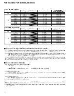
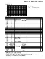
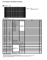
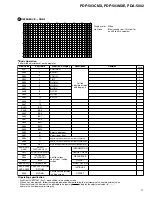
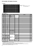
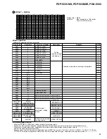
OFFSET — RGB2

2

:

Display color : White
Half tone

: Blue (second row / 15th row for 
   each 5 to 36th columns)

Perform the adjustment of each parameter.

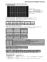
Basic Operation

Operating specification

• Start from CONTRAST (key 1) when shifted to this setting screen.
• When a key was pressed, follow the required operation after performing the last memory of current adjustment value.
• When there is not the item which is applicable to an input signal mode, display the adjustment value to "

−−−−−

 (

−−−−−

)",

and turn the item display color into gray.

Summary of Contents for PDA-5002

Page 1: ...LODED VIEWS AND PARTS LIST 6 3 BLOCK DIAGRAM AND SCHEMATIC DIAGRAM 26 For SCHEMATIC DIAGRAM refer to ARP3100 4 PCB CONNECTION DIAGRAM Refer to ARP3100 5 PCB PARTS LIST 50 6 ADJUSTMENT 66 CONTENTS 7 GENERAL INFORMATION 126 7 1 DIAGNOSIS 126 7 1 1 PCB LOCATION 126 7 1 2 SHUT DOWN POWER DOWN DIAGNOSIS BY LED DISPLAY 127 7 1 3 AUTOMATIC BACKUP OF DIGITAL VIDEO ASSY DATA 136 7 1 4 DISASSEMBLY 138 7 2 I...

Page 2: ...apacitor etc 3 When service is required observe the original lead dress Extra precaution should be taken to assure correct lead dress in the high voltage circuitry area 4 Always use the manufacture s replacement components Especially critical components as indicated on the circuit diagram should not be replaced by other manufacture s Furthermore where a short circuit has occurred replace those com...

Page 3: ...urrent measured must not exceed 0 5mA ANY MEASUREMENTS NOT WITHIN THE LIMITS OUTLINED ABOVE ARE INDICATIVE OF A POTENTIAL SHOCK HAZARD AND MUST BE CORRECTED BEFORE RETURNING THE SET TO THE CUSTOMER 1 2 PRODUCT SAFETY NOTICE Many electrical and mechanical parts in PIONEER set have special safety related characteristics These are often not evident from visual inspection nor the protection afforded b...

Page 4: ...ransformer In the SW POWER SUPPLY Module 6 Other primary side of the SW POWER SUPPLY Module 1 3 CHARGED SECTION AND HIGH VOLTAGE GENERATING POINT 7 High Voltage Generating Point The places where voltage is 100V or more except for the charged places described above If the places are touched there is a risk of electric shock 1 SW POWER SUPPLY Module 225V 2 X DRIVE Assy 300V to 225V 3 Y DRIVE Assy 35...

Page 5: ...5 PDP 503CMX PDP 503MXE PDA 5002 ...

Page 6: ... The mark found on some component parts indicates the importance of the safety factor of the part Therefore when replacing be sure to use parts of identical designation Screws adjacent to mark on the product are used for disassembly 1 2 3 3 9 10 11 2 26 5 4 8 7 12 11 31 32 33 16 17 18 19 20 21 22 30 25 24 23 27 28 35 6 29 36 PDP 503MXE Only PDP 503MXE Only 15 PDP 503CMX Only PDP 503CMX Only PDP 50...

Page 7: ...5 Warranty Card ARY1102 NSP 26 Vinyl Pouch See Contrast table 2 27 Washer WB80FZB 28 Hex Hole Bolt SMZ80H400FZB 29 Vinyl Bag AHG 064 30 Caution Sheet See Contrast table 2 31 Remote Control Unit AXD1459 32 Battery Cover AZN2462 NSP 33 Dry Cell Battery R6P AA AEX1026 34 Display Stand AMR3264 35 Remote Control Unit Holder AMR3268 36 Ferrite Core See Contrast table 2 2 CONTRAST TABLE PDP 503CMX LUCB a...

Page 8: ... AWZ6650 2 CLAMP B Assy AWZ6651 3 CLAMP C Assy AWZ6652 4 CLAMP D Assy AWZ6653 5 Service Panel Assy AWU1040 UNDER LAYER SECTION 1 PARTS LIST Mark No Description Part No Mark No Description Part No 6 Wire Saddle AEC1878 7 Circuit Board Spacer AEC1872 8 Circuit Board Spacer AEC1873 NSP 9 PCB Spacer AEC1253 10 Locking Card Spacer AEC1736 11 Screw ABA1301 12 V Cushion AED1205 ...

Page 9: ...nd Wire Saddle AEC1878 as follows Therefore need to remove it in accordance with model Confirm character carved a seal near the parts and remove it P Public exclusive use W Module exclusive use PW Common use of public use and module In case of this unit all the parts carved a seal of character removes it Wire Saddle AEC1878 Service Panel Assy AWU1040 Circuit Board Spacer AEC1872 Circuit Board Spac...

Page 10: ... Assy AWZ6626 2 ADR CONNECT B Assy AWZ6627 3 ADR CONNECT C Assy AWZ6628 4 ADR CONNECT D Assy AWZ6629 5 BRIDGE A Assy AWZ6620 UNDER LAYER SECTION 2 PARTS LIST Mark No Description Part No Mark No Description Part No 6 BRIDGE B Assy AWZ6621 7 BRIDGE C Assy AWZ6622 8 BRIDGE D Assy AWZ6623 9 RESONANCE Assy AWZ6630 10 Screw ABA1301 11 Screw VBB30P100FNI ...

Page 11: ...PDP 503CMX PDP 503MXE PDA 5002 11 Upper side Upper side 3 7 3 19 13 12 12 21 7 12 11 14 5 10 10 4 9 7 8 8 6 17 15 6 16 1 18 2 25 22 24 13 13 13 13 26 13 13 24 24 13 2 1 4 UNDER LAYER SECTION 3 ...

Page 12: ...er AEC1872 12 Screw ABZ30P060FMC 13 Screw VBB30P100FNI 14 Screw PMB30P060FNI 15 J201 Flexible Flat Cable ADD1183 UNDER LAYER SECTION 3 PARTS LIST Mark No Description Part No Mark No Description Part No 16 J202 Flexible Flat Cable ADD1183 17 J209 Flexible Flat Cable ADD1191 18 J204 Flexible Flat Cable ADD1196 19 J210 Flexible Flat Cable ADD1190 20 J211 Flexible Flat Cable ADD1186 21 J212 Flexible F...

Page 13: ...ark No Description Part No Mark No Description Part No 11 Scan IC Spring L ABK1026 12 Scan IC Spring R ABK1027 13 Scan Insulation Sheet AMR3271 14 Rivet BEC1066 15 Circuit Board Spacer AEC1872 16 Screw ABZ30P060FMC 17 Screw PMB30P060FNI 18 Screw VBB30P100FNI 19 J208 Flexible Flat Cable ADD1191 20 J207 Flexible Flat Cable ADD1190 21 J203 Flexible Flat Cable ADD1184 22 J205 Flexible Flat Cable ADD11...

Page 14: ...sy AWZ6646 3 SUB ADDRESS B Assy AWZ6647 4 Circuit Board Spacer AEC1873 5 Power Sheet AMR3291 6 Rivet BEC1066 7 Fan Label AAX2785 NSP 8 Fan Metal ANG2465 9 Fan Motor AXM1040 10 Screw PPZ50P100FZK 11 Screw ABZ30P060FMC NSP 12 Heatsink ANH1594 13 Silicone Sheet AEH1039 2 1 6 UNDER LAYER SECTION 5 UNDER LAYER SECTION 5 PARTS LIST Mark No Description Part No ...

Page 15: ...ER LAYER SECTION 6 UNDER LAYER SECTION 6 PARTS LIST Mark No Description Part No Mark No Description Part No 21 V MID CLAMP Assy AWV1934 22 Flat Clamp AEC1879 23 J115 3P Housing Wire ADX2705 24 J110 3P Housing Wire ADX2704 25 J108 8P Housing Wire ADX2701 26 J101 Wire F ADX2695 27 J102 Wire E ADX2694 28 J103 13P Housing Wire ADX2700 29 J116 4P Housing SP Wire ADX2725 30 J109 Wire G ADX2696 31 J111 W...

Page 16: ... ANG2455 NSP 5 Sub Frame R ANG2456 6 FPC Cushion AEB1370 NSP 7 Front Chassis V ANA1661 8 Screw ABA1283 9 Screw ABA1294 10 Screw BMZ30P060FMC 11 V Cushion AED1205 2 1 8 MIDDLE LAYER SECTION 1 MIDDLE LAYER SECTION 1 PARTS LIST Mark No Description Part No 1 9 9 9 10 10 9 9 9 9 9 8 8 9 9 11 7 7 11 11 6 11 5 3 3 7 4 9 8 9 9 1 2 8 7 6 6 ...

Page 17: ...2699 4 KEY CONNECTOR Assy AWZ6638 NSP 5 IR Holder ANG2494 6 Nyron Rivet AEC1671 7 J111 Wire I ADX2698 NSP 8 Switch Holder ANG2493 9 Screw BMZ30P040FMC 10 Screw ABZ30P050FZK 2 1 9 MIDDLE LAYER SECTION 2 MIDDLE LAYER SECTION 2 PARTS LIST Mark No Description Part No 3 7 2 9 9 4 5 1 9 8 10 10 6 6 ...

Page 18: ...round Finger ANG2468 7 Card Spacer AEC1899 8 Ferrite Core L3 ATX1037 9 Ferrite Core Holder AEC1818 10 NSP 11 Guide Rail EX BEC1185 12 Clamp AEC1884 13 J107 12P Housing Wire ADX2702 14 J109 Wire G ADX2696 15 Nyron Rivet AEC1671 16 J111 Wire I ADX2698 17 Wire Saddle AEC1745 NSP 18 Video Stay AND1171 19 20 NSP 21 PCB Stay AND1170 22 Screw AMZ30P060FZK 23 Screw VBB30P100FNI 2 1 10 MIDDLE LAYER SECTION...

Page 19: ...2 2 Slot Spring Under ABK1028 3 Slot Spring Upper ABK1024 4 Card Spacer AEC1898 5 Enclosure Sheet AMR3281 6 Screw AMZ30P060FZK 7 Screw TBZ40P080FZK 8 Rear Corner Label AAX2862 9 Expansion Slot Cover ANG2463 10 Screw BMZ30P060FZK 2 1 11 MIDDLE LAYER SECTION 4 MIDDLE LAYER SECTION 4 PARTS LIST Mark No Description Part No ...

Page 20: ...PDP 503CMX PDP 503MXE PDA 5002 20 2 1 12 UPPER LAYER SECTION 1 16 J201 J201 J201 J202 7 1 15 J113 9 2 C3 C1 12 13 11 10 2 5 3 18 17 6 4 14 15 14 17 17 18 ...

Page 21: ...th Filter CN1 AKP1223 7 J201 J202 Flexible Cable ADD1183 8 9 J109 Wire G ADX2696 10 J106 Wire C ADX2693 11 Ferrite Core L1 ATX1032 12 J114 Earth Wire ADX2709 13 J105 Wire B ADX2692 14 Hexagonal Nut ABN1035 15 Hexagonal Head Screw BBA1051 16 Screw PMB30P060FNI 17 Screw BPZ30P080FZK 18 Screw BMZ30P060FZK UPPER LAYER SECTION 1 PARTS LIST Mark No Description Part No ...

Page 22: ... 1 SW Power Supply Module AXY1053 2 Ferrite Core L3 ATX1037 3 Ferrite Core L2 ATX1039 4 Binder AEC 093 5 J105 Wire B ADX2692 6 J102 Wire E ADX2694 7 J103 13P Housing Wire ADX2700 8 J112 13P Housing Wire ADX2703 9 J101 Wire F ADX2695 10 J104 Wire H ADX2697 11 J111 Wire I ADX2698 12 Screw AMZ30P060FZK UPPER LAYER SECTION 2 PARTS LIST Mark No Description Part No ...

Page 23: ...99 14 Panel Cushion H AED1198 15 Protect Panel Assy AMR3266 16 Screw ABZ30P050FZK 17 Screw VMZ30P060FZK 18 Energy Star Label AAX2856 19 Display Label See Contrast table 2 FRONT CASE SECTION PARTS LIST Mark No Description Part No 2 18 3 17 8 10 10 10 16 16 7 6 5 4 1 19 10 11 10 16 13 13 15 14 14 16 16 10 9 10 16 10 11 11 11 PDP 503CMX Only 2 CONTRAST TABLE PDP 503CMX LUCB and PDP 503MXE YVLDK are c...

Page 24: ...UKUGO ASSY AWV1898 ADDRESS FUKUGO ASSY AWV1900 NSP Address Module IC1 IC40 AXF1110 NSP FPC 0003 ADY1065 NSP FPC J0001 ADY1066 NSP Chassis ANA1655 NSP Base Chassis ANA1656 NSP Scan Heatsink ANH1595 NSP Corner Angle A ANG2457 NSP Corner Angle B ANG2458 NSP Tube Cover AMR3262 Siricon Sheet 50 AEH1037 Adhesive Tape 50 AEH1038 Adhesive Tape B 50 AEH1051 Pin Grommet AEC1015 Card Spacer AEC1889 Scan Siri...

Page 25: ...AIN UNIT 1 VIDEO SLOT ST1 Assy AWV1906 2 Video Terminal Panel M ANG2461 3 Screw ABA1295 4 Hexagonal Head Screw BBA1051 5 Screw BPZ30P080FZK 6 Rivet AEP 211 7 Sheet AMR3282 5 3 3 4 6 1 2 7 Mark No Description Part No NSP 5 Vinyl Bag AHG 064 6 Operating Instructions ARC1504 Spanish Italian Dutch 7 Operating Instructions ARD1043 Japanese English French German NSP 8 Warranty Card ARY1093 9 Connector I...

Page 26: ...2V 13 5V 9V 6 5V STB5V 12V STB5V 12V 13 5V 9V 6 5V STB5V IN1 DET C1 R6 R2 R3 3ST REG RE 3V 5V 3V R4 R9 AC1 L OUT K2 60 C3 SPR1 KL2 KL1 RE1 SW1 TE1 DIGITAL ASSY Y DRIVE ASSY POWER SUP THERMAL SENSOR ASSY ADR RESONANCE ASSY ADDRESS CONNECT B ASSY ADDRESS CONNECT A ASSY ADR RESONANCE ASS RGB ASSY K2 ADDRESS CONNECT D ASSY ADDRESS CONNECT C ASSY CLAMP C ASSY BRIDGE C ASSY BRIDGE A ASSY CONTROL ASSY SP...

Page 27: ... DET 3STATE Buffer AWV1906 Only IN3 DET OUTPUT INPUT3 INPUT4 INPUT 5 REG REG 7V 8V 7V 3V 5V 5V 3V 5V 6M LPF 3D Y C CNR I2C BUS R4 R9 R1 R8 A5 A1 A6 A7 A3 I2C BUS AB1 AA1 L OUT V MID CLAMP U V MID CLAMP L VM2 VM1 K3 2 60 SPL1 L1 POWER SUPPLY MODULE SUB ADDRESS A ASSY ADDRESS CONNECT C ASSY ADDRESS CONNECT D ASSY MX AUDIO ASSY VIDEO SLOT ST1 ASSY SLOT CONNECTOR ASSY V MID CLAMP ASSY X DRIVE ASSY X C...

Page 28: ...LPF CLP_MAT CLP_AMP CLP_AMP HOLD IC4402 CXA2101AQ MATRIX 35M 3 1 Select IC4603 CXA3516R A D PLL AMP 2 1 Select IC5001 IC102 IC5102 PE5066ACK IC101 LCX125 CLK SEL SD RAM 16M SD RAM 16M SCP IN 31 HOLD 106 G YOUT 2 B CbOUT 1 R_CrOUT 3 SYNCIN 111 112 CLPIN 113 XUNLOCK 104 1 2CLK 101 DIVOUT 103 SDA 56 SCL 55 ACL AMP ACL I O ASSY LCX541 2 1 Selector Buffer Clamp SW DIVOUT 32 HD_SEP 106 VD_SEP 107 CLP_SE...

Page 29: ...UTE 60 WE_MD 72 RXD0 36 TXD0 35 TEMP2 95 BUSY30 55 RESET 61 WAIT_FLASH 102 A13_FLASH 70 CS_FLASH 69 RY BY 102 WACT_FRCT 32 HD_W 117 VD_W 34 73 DE_W 33 72 H 119 VI 31 FI 118 CS_30 66 IC_RST 126 RDB 91 HWRS 92 SGLB_AD 79 HWR_30 φ 88 D_CLK 63 D_RXD 61 WU_CE 29 FEW_CE 60 MD2 125 EXT_RXD 62 EXT_TXD 60 REQ_WU 71 D_BUSY 64 DLK_PLL 105 PLL_OE 33 TXD_WU 97 SCK_WU 101 RST2 75 IN5DET 49 BUSY 54 REQ_WU 74 WE_...

Page 30: ...ft section ADR CONNECT A D Assy Right section Y DRIVE Assy X DRIVE Assy RESONANCE Assy 5V 5V PC_VIDEO ADR_K_EMG STOPB 3 3V 3 3V 12V ADR K PD U ADR PD APD MUTE EXD TXD RST2 RST PU EXD RXD RESET RESET RXD BUSY REQ_PU ADR K PD D DEW DET RELAY TEMP1 STB5V STB5V STB5V 3 3V 2 5V 3 3V 3 3V 3 3V VD HD VD 31 APLR STB5V 2 5V IIC BUS RGB 2 phase 10 bit VD HD DE CLK Address BUS Data BUS Control Signal RXDO RE...

Page 31: ...95 460 Pulse Module IC3201 STK795 460 Pulse Module T3701 VRN D D CONV XCP MSK XSUS MSK VCP PLD SUSOUT A 37 40 29 30 K3105 PSUS K3107 IC3103 IC3104 TND301S Q3103 Q3107 Q3104 Q3109 Q3105 Q3124 Q3106 Q3125 SUSOUT B 37 40 29 30 K3106 IC3106 IC3107 TND301S Q3110 Q3114 Q3111 Q3115 Q3112 Q3126 Q3113 Q3127 To X CONNECTOR ASSY IC3110 TND301S IC3113 TND301S charge pump circuit From DIGITAL VIDEO ASSY Photo ...

Page 32: ...1 IC2006 PE1013 IC2005 TC74ACT541FT Dew DET circuit Photo Coupler OC2 2 Y3 Y5 Photo Coupler SUS muteDET circuit charge pump circuit Photo Coupler VOFS D D CONV D GND 13 5V SUSGND D GND IC5V VF D D CONV IC5V UVP VOFS UVP VOFS OVP VH UVP VH OVP VOFS VF IC5V VF VH YSOFT D YOFS YCP MSK VH VH IC5V 13 5V 9V IC2208 HCPL M611 IC2001 TC74ACT541FT Q2102 IC2504 TC74ACT540FT IC2506 TC74ACT540FT IC2503 TC74ACT...

Page 33: ...9 30 29 30 IC2201 TC74ACT541FT K2212 K2203 K2220 PSUS IC2212 TND301S Q2219 Q2218 IC2213 TND301S 2 9 11 18 Q2215 Q2216 Q2217 Q2226 IC2217 TND301S Q2227 Q2220 Q2221 Q2228 Q2232 Q2233 IC2216 TND301S YPR U1 YPR U2 VSUS SUSGND Q2210 Q2211 Q2212 Q2204 Q2205 IC2203 TND301S IC2204 TND301S IC2210 TND301S Vsus 15V 5V Vsus 15V 5V ...

Page 34: ... R_Audio GND A_Mute Stand_by GND L_Audio R_Audio L_Audio 5VSTB R_OUT R_GND L_GND L_OUT Temp3 POWER AMP IC8601 15V 5VSTB D C Detect FAN_PD FAN_D FAN_PD FAN_D 15V Vin Vout Vc Vadj FAN_Mute 3 4V REGULATOR IC8701 5V_AD RGB Audio_NG Temp3 FAN_NG uCOM_FAN OP AMP Buf 5V_AD RGB 5V_AD RG B NOR 3 06V 1 66V Audio Mute A5 A1 A6 A7 A3 ...

Page 35: ...IC8801 D8804 DC AC AC 5V SW ADR D DC CLK ADR U ADR B 12V IC8802 IC8802 IC8803 DGND VADR ADRGND CLR ADROUT CN8803 IC8804 Current Voltage Convert Block Over Current DET Block ADR Output Resistance Load Block P D Output Block BUFF Block Inversion Block Additional Block Conparator EMG ON Flip Flop 5V REG H EMG1 OFF L EMG1 ON H V MID CLAMP OFF L V MID CLAMP ON Conparator EMG OFF 3 1 7 SUB ADDRESS A and...

Page 36: ...B C6721 Q6708 ADR U Q6709 ADR D SW CN6701 ADR OUT L6704 IC6702 Q6702 Q6705 VADR V MID ADR D ADRGND C6722 Q6710 DGND Q6711 SW CN6703 DGND IC6703 Q6703 Q6712 V MID C6716 C6718 ADRGND ICP S1 0 ADR B Pre Drive ADR U Pre Drive ADR U Drive ADR D Pre Drive ADR D Drive ADR B Drive CAUTION FOR CONTINUED PROTECTION AGAINST RISK OF FIRE REPLACE ONLY WITH SAME TYPE NO ICP S1 0 MFD BY ROHM CO LTD FOR IC6704 3 ...

Page 37: ...DATA_G DATA_B DATA_R DATA_G DATA_B DATA_R DATA_G DATA_B DATA_R DATA_G DATA_B DATA_R DATA_G DATA_B HZ LBLK HBLK LE CLK V MID CLAMP U Output Block D9010 VADR U V MID U ADRGND U Q9006 NC DGND U NC SW U CN9002 R9012 Q9002 Q9004 R9014 V MID CLAMP L Output Block D9019 VADR L V MID L ADRGND L Q9005 DGND L SW L CN9001 R9011 Q9001 Q9003 R9013 V MID CLAMP Reference Voltage Block V MID CLAMP Reference Voltag...

Page 38: ...6 Input 5 DVI D Terminal In DVI_PS Input5 SELECT Hi OTHERS Lo Hi Normal Operation Lo Power Down PLK_CNT 0 4 CLK_PLK IC7307 pin 7 No 10 11 HD_PLK IC7307 pin 7 No 9 12 DE_PLK IC7307 pin 7 No 9 11 VD_PLK IC7307 pin 5 No 9 12 RB_PLKO4 IC7407 pin 15 No 10 11 IC7002 NJM2234M 2 Selector IC7101 ML6428CS 1 6M LPF IC7003 TC4052BF 2 1 Selector JA7004 DKB1031 Input 3 Audio In IC7001 TK15420M Video Driver IC71...

Page 39: ...LPF IC4403 IC4402 CXA2101AQ IC5001 PE5067A K IC4603 CXA3516R IC4108 BA7657F IC5301 PD6357B IC4108 BA7657F 6M LPF IC4403 IC4402 CXA2101AQ IC4603 CXA3516R IC5001 PE5067A K IC5301 PD6357B IC4108 BA7657F IC4402 CXA2101AQ IC4603 CXA3516R IC5001 PE5067A K IC5301 PD6357B IC4108 BA7657F IC4603 CXA3516R IC5001 PE5067A K IC5301 PD6357B IC4402 CXA2101AQ IC4603 CXA3516R IC5001 PE5067A K IC5301 PD6357B IC5301 ...

Page 40: ...4108 BA7657F IC5301 PD6357B INPUT1 INPUT2 INPUT3 4 INPUT5 IC4803 PDY077 IC4108 BA7657F IC4801 NJM2234 IC4802 M52346SP IC5001 PE5067A K IC5301 PD6357B IC4108 BA7657F IC4803 PDY077 IC5001 PE5067A K IC5301 PD6357B IC4802 M52346SP IC4108 BA7657F IC5001 PE5067A K IC5301 PD6357B IC4803 PDY077 IC5001 PE5067A K IC5301 PD6357B IC4803 PDY077 IC4803 PDY077 IC4801 NJM2234 IC4802 M52346SP IC5001 PE5067A K IC53...

Page 41: ... div 6 CH1 IC5505 pin 1 TXD CH2 IC5505 pin 2 CLK V 5V div H 100µsec div 7 IC5505 pin 15 XIN V 2V div H 50nsec div 3 IC5505 pin 20 KEYSCAN V 5V div H 50msec div 4 IC5505 pin 35 TXDO V 5V div H 1msec div 5 IC5505 pin 18 REM V 5V div H 50msec div GND GND GND GND GND CH1 CH1 CH2 CH2 GND GND GND GND GND GND GND GND GND GND GND GND GND GND CH1 CH1 CH1 CH1 CH2 CH2 CH2 CH2 3 2 WAVEFORMS ...

Page 42: ...8 YSUS_B V 2V div H 2msec div 7 K1308 VDRB R1343 pin 8 RDAT_DL0 V 2V div H 4msec div 8 K1308 VDRB IC1501 pin 15 LBLK V 2V div H 2msec div 9 K1308 VDRB IC1501 pin 13 LE V 2V div H 2msec div 10 IC1501 pin 13 LE IC1501 pin 11 ADRCLK V 2V div H 200nsec div 10 IC1501 pin 13 LE IC1501 pin 11 ADRCLK V 2V div H 20nsec div 1 K1327 VDI K1328 HDI V 2V div H 10µsec div 2 K1327 VDI CN1004 pin 49 R DIGITAL VIDE...

Page 43: ...2msec div Input VIDEO Signal Color bar 1 CH1 IC8801 pin 3 CH2 IC8801 pin 7 CH3 IC8802 pin 1 V 2V div H 2msec div Input VIDEO Signal Color bar CH1 H 2msec div CH2 CH3 V MID CLAMP ASSY 2 CH1 Q9006 Base CLAMP REF V CH2 D9010 Anode MID CH3 Q9006 Collector V 10V div H 2msec div Input PC Signal Color bar 1 CH1 Q9006 Base CLAMP REF V CH2 D9010 Anode MID CH3 Q9006 Collector V 10V div H 2msec div Input VID...

Page 44: ... RAMP 10 CH1 IC7408 pin 18 CLK_PLK CH2 IC7408 pin 15 HD_PLK CH3 IC7408 pin 17 DE_PLK CH4 IC7408 pin 15 RB_PLKO4 V 5V div H 10µsec div INPUT5 VESA 1024 768 60Hz RAMP 11 CH1 IC7408 pin 18 CLK_PLK CH2 IC7408 pin 15 HD_PLK CH3 IC7408 pin 17 DE_PLK CH4 IC7408 pin 15 RB_PLKO4 V 5V div H 40nsec div INPUT5 VESA 1024 768 60Hz RAMP 12 CH1 IC7408 pin 14 VD_PLK CH2 IC7410 pin 5 VD_PLKU CH3 IC7408 pin 15 HD_PL...

Page 45: ...n Mode FULL Clamp Mode AUTO Color Mode COLOR MODE 1 28 29 to Input INPUT 5 DVI Input Signal XGA 60Hz Signal Pattern Monoscope Screen Mode FULL Clamp Mode AUTO Color Mode COLOR MODE 1 30 31 to Input INPUT 2 RGBHV Input Signal 1125i Signal Pattern Monoscope Screen Mode FULL Clamp Mode AUTO Color Mode COLOR MODE 1 32 33 IC4108 BA7657F IC4402 CXA2101AQ IC4403 6MLPF IC4603 CXA3516R IC5301 PD6357B IC500...

Page 46: ...13 T2 23 CN5702 pin 28 Synchronize with IC4802 pin 13 T2 24 IC4803 pin 139 Synchronize with IC4802 pin 13 T2 25 K4806 Synchronize with IC4802 pin 13 T2 26 IC4402 pin 31 Synchronize with IC4802 pin 13 T2 27 K4603 Y_SIGNAL Synchronize with IC4802 pin 13 T2 28 K5314 DE_SEL K5314 DE_SEL is fixed to L level in the PC signal indication K5315 HD_SEL and k 5317 HD _ 30 synchronize with K5316 VD_SEL K5316 ...

Page 47: ...iv T1 8 IC4802 pin 4 V 2V div H 10µsec div T1 9 IC4802 pin 15 V 2V div H 10µsec div T1 10 IC4402 pin 31 V 2V div H 10µsec div T1 11 IC4603 pin 113 V 2V div H 10µsec div T1 12 IC4603 pin 103 V 2V div H 10µsec div T1 13 IC4603 pin 101 V 2V div H 10µsec div T1 14 IC4603 pin 98 V 2V div H 80msec div T1 15 K5315 V 2V div H 10µsec div T1 16 CN5702 pin 26 V 2V div H 10µsec div T1 17 K5315 V 2V div H 10µs...

Page 48: ...3 K5314 DE_SEL K5315 HD_SEL K5316 VD_SEL K5317 HD_30 V 5V div H 200µsec div 27 K4603 Y_SIGNAL V 1V div H 20µsec div 28 K5314 DE_SEL K5315 HD_SEL K5316 VD_SEL K5317 HD_30 V 5V div H 2msec div 29 K5314 DE_SEL K5315 HD_SEL K5316 VD_SEL K5317 HD_30 V 5V div H 40µsec div 31 K5314 DE_SEL K5315 HD_SEL K5316 VD_SEL K5317 HD_30 V 5V div H 100µsec div 30 K5314 DE_SEL K5315 HD_SEL K5316 VD_SEL K5317 HD_30 V ...

Page 49: ...iv H 5µsec div Sustain Waveform sustain ch 1 K3107 X PSUS K3201 SUSGND V 50V div H 2µsec div ch 2 K2220 Y PSUS K2219 SUSGND V 50V div H 2µsec div Sustain Waveform reset pulse ch 1 K3107 X PSUS K3201 SUSGND V 100V div H 5µsec div ch 2 K2220 Y PSUS K2219 SUSGND V 100V div H 5µsec div Y Drive Pulse Control Waveform 1 field ch 1 K2220 Y PSUS K2219 SUSGND V 100V div H 2msec div ch 2 K2039 YCP_MSK K2024...

Page 50: ...DGE C ASSY AWZ6622 NSP BRIDGE D ASSY AWZ6623 NSP CLAMP A ASSY AWZ6650 NSP CLAMP B ASSY AWZ6651 NSP CLAMP C ASSY AWZ6652 NSP CLAMP D ASSY AWZ6653 ADDRESS FUKUGO ASSY AWV1900 NSP ADR CONNECT A ASSY AWZ6626 NSP ADR CONNECT B ASSY AWZ6627 NSP ADR CONNECT C ASSY AWZ6628 NSP ADR CONNECT D ASSY AWZ6629 NSP RESONANCE ASSY AWZ6691 X DRIVE ASSY AWV1901 Y DRIVE ASSY AWV1902 SLOT CONNECTOR ASSY AWZ6634 Y DRIV...

Page 51: ...EST PIN AKX9002 X CONNECTOR A ASSY RESISTORS R6401 RS1 16S0R0J X CONNECTOR B ASSY RESISTORS R6451 RS1 16S0R0J BRIDGE A ASSY SEMICONDUCTORS D6421 D6422 D1FL20U S CAPACITORS C6421 C6422 0 1µF 100V ACG1098 OTHERS CN6421 PH CONNECTOR B4B PH SM3 BRIDGE B ASSY SEMICONDUCTORS D6431 D6432 D1FL20U S CAPACITORS C6431 C6432 0 1µF 100V ACG1098 OTHERS CN6431 PH CONNECTOR B4B PH SM3 BRIDGE C ASSY SEMICONDUCTORS...

Page 52: ...1 C6625 C6632 CKSRYF104Z16 C6635 CKSRYF104Z16 RESISTORS R6618 R6622 R6624 R6626 R6628 RAB4C100J R6630 R6631 R6633 R6637 R6639 RAB4C100J R6641 R6643 R6645 R6647 RAB4C100J R6616 RAB4C473J Other Resistors RS1 16S J OTHERS CN6601 55P CONNECTOR AKM1202 ADR CONNECT C ASSY SEMICONDUCTORS IC6801 TC74VHC541FT Q6802 2SC2712 Q6803 2SK209 D6801 DA227 COILS L6801 L6802 22µH 0 11A ATH1081 CAPACITORS C6811 C6820...

Page 53: ...1 K3003 K3004 K3008 K3010 AKX9002 TEST PIN K3012 K3015 K3017 K3018 AKX9002 TEST PIN CN3001 30P CONNECTOR KF050HA30L X SUS BLOCK SEMICONDUCTORS IC3102 HCPL M611 IC3200 IC3201 STK795 460 IC3101 TC74ACT541FT IC3103 IC3104 IC3106 IC3107 TND301S IC3110 IC3113 TND301S IC3109 UPC78L05T Q3117 2SJ181L Q3116 Q3119 Q3120 2SJ522 Q3101 2SK2503 Q3103 Q3107 Q3109 Q3115 FS16VS 9 Q3124 Q3127 FS16VS 9 Q3123 FS2AS 1...

Page 54: ...10 CKSRYB104K16 C3715 C3716 CKSRYB104K16 RESISTORS R3732 RS1 16S1001F R3806 RS1 16S1802F R3701 R3704 R3706 R3717 RS1 16S1803F R3805 RS1 16S2702F R3731 RS1 16S3900F R3802 RS1 16S5601F R3738 R3739 RS1 2S102J R3800 R3801 RS1 2S823J VR3701 1kΩ ACP1089 Other Resistors RS1 16S J OTHERS T3701 VRN TRANSFORMER ATK1153 SCREW PMB30P060FNI Y DRIVE ASSY Y DRIVE LOGIC BLOCK SEMICONDUCTORS IC2006 PE1013A IC2007 ...

Page 55: ...2361 RS1 16S3300F R2263 R2264 RS1 2S100J R2203 RS1 2S102J R2209 RS1 2S2R2J R2202 RS1 2S561J R2278 R2303 RS1MMF101J R2233 R2234 RS1MMF102J R2274 R2275 RS1MMF221J R2298 R2299 RS2MMF4R7J R2277 RS3PMFR47J R2276 RS3PMFR56J VR2201 VR2204 1kΩ ACP1089 Other Resistors RS1 16S J OTHERS SPACER AEH1049 K2211 K2214 K2217 TEST PIN AKX9002 KN2201 KN2210 GROUND PLATE ANK 142 CN2201 15P PLUG KM250MA15 CN2202 3P PL...

Page 56: ... J OTHERS T2702 SMD TRANSFORMER ATK1150 T2703 VH TRANSFORMER ATK1151 T2701 VOFS TRANSFORMER ATK1152 SCREW PMB30P060FNI SLOT CONNECTOR ASSY OTHERS CN8102 SOCKET 120P AKP1219 CN8101 PCI SOCKET 120P AKP1220 KN8101 KN8102 GROUND PLATE ANK1664 SUB ADDRESS A ASSY SEMICONDUCTORS IC8801 IC8802 IC8804 M5223AFP IC8803 TC74VHC74FT Q8801 Q8802 2SA1163 Q8803 Q8805 Q8808 2SC2712 Q8806 2SK209 D8801 D8803 D8809 1...

Page 57: ... IC1101 HD64F2328VF IC1103 NC7SZ08P5 IC1102 PST9228N Q1101 Q1103 DTC143EK D1101 AEL1171 CAPACITORS C1123 C1124 CCSRCH7R0D50 C1101 CEV101M4 C1102 C1109 C1110 C1112 C1116 CKSRYB102K50 C1129 C1132 CKSRYB102K50 C1117 C1121 CKSRYB103K50 C1120 CKSRYB472K50 C1103 C1108 C1111 C1118 C1119 CKSRYF104Z16 C1122 C1125 C1128 CKSRYF104Z16 RESISTORS R1104 R1107 R1110 R1113 R1114 RAB4C472J R1116 R1121 R1124 R1127 R...

Page 58: ...CONNECTOR K1301 K1302 K1308 K1311 K1314 AKX9002 TEST PIN K1316 K1321 K1324 K1326 K1331 AKX9002 TEST PIN K1333 K1501 K1502 K1601 K1602 AKX9002 TEST PIN K1728 K1729 TEST PIN AKX9002 X1801 CRYSTAL RESONATOR ASS1146 50 000MHz CN1503 CN1603 PH CONNECTOR B8B PH SM3 CN1301 8P PLUG CKS3130 CN1702 30P CONNECTOR KF050HA30L D D CONVERTER BLOCK SEMICONDUCTORS Q1902 Q1905 Q1907 2SC2712 Q1903 DTC143EK Q1901 Q19...

Page 59: ...CN4104 D SUB SOCKET AKP1214 CN4105 BNC SOCKET AKX1055 RGB ASSY MATRIX BLOCK SEMICONDUCTORS IC4402 CXA2101AQ IC4403 ML6426CS 1 IC4404 NJM072BM E Q4407 Q4409 2SA1037K Q4413 2SC2412K Q4412 HN1A01FU Q4404 HN1B04FU Q4410 HN1C01FU D4401 1SS226 CAPACITORS C4406 C4412 C4458 CEHAT100M50 C4405 CEHAT101M16 C4456 CEHAT470M16 C4437 C4451 C4453 CKSQYB105K10 C4407 C4409 C4410 C4428 C4429 CKSQYB474K16 C4431 C4432...

Page 60: ...C4813 C4814 CKSRYF104Z16 C4819 C4820 C4830 C4831 C4836 CKSRYF104Z16 C4839 C4842 C4843 C4850 C4861 CKSRYF104Z16 C4860 CKSRYF105Z10 RESISTORS R4814 R4818 R4835 R4915 RAB4C101J R4913 RAB4C102J R4809 RAB4C152J R4825 RAB4C471J R4808 R4943 RAB4C472J R4864 RS1 16S1802F R4865 RS1 16S2702F R4868 RS1 16S4702F Other Resistors RS1 16S J OTHERS K4801 K4802 K4805 K4806 AKX9002 TEST PIN K4809 K4810 TEST PIN AKX9...

Page 61: ...1204 K5501 K5502 K5508 K5510 K5512 AKX9002 TEST PIN K5515 K5516 K5518 TEST PIN AKX9002 X5501 CERAMIC RESONATOR ASS1159 16MHz CN5501 CN5502 8P PLUG CKS3130 WIDE UCOM BLOCK SEMICONDUCTORS IC5601 HD64F2328VF IC5604 NC7SZ08P5 IC5603 PST9228N IC5605 TC7SH32FU IC5607 IC5608 TC7WH74FU CAPACITORS C5601 CCSRCH102J50 C5615 C5616 CCSRCH7R0D50 C5611 CKSRYB472K50 C5612 CKSRYF103Z50 C5604 C5606 C5608 C5610 C561...

Page 62: ... D8010 1SS355 D8001 D8008 UDZ15B COIL L8001 LCTA221J3225 CAPACITORS C8001 C8002 C8005 C8006 CEAT1R0M50 C8003 C8010 CEAT470M16 C8004 C8007 C8008 CKSRYB103K50 C8009 CKSRYB472K50 RESISTORS R8006 RAB4C102J Other Resistors RS1 16S J OTHERS CN8001 CN8002 MINI JACK AKN1070 CN8003 9P D SUB SOCKET AKP1213 CN8004 CN8005 AKP1215 6P MINI DIN SOCKET CN8007 PH CONNECTOR B6B PH SM3 SP OUT L ASSY SEMICONDUCTORS I...

Page 63: ...SSY SEMICONDUCTORS D8501 AEL1170 OTHERS CN8501 PH CONNECTOR S3B PH SM3 IR ASSY SEMICONDUCTORS Q8551 2SC2712 D8552 1SS226 D8551 1SS355 CAPACITORS C8551 CEV470M6R3 C8553 CKSQYB472K50 C8552 CKSRYB103K50 C8554 CKSRYF104Z16 RESISTORS All Resistors RS1 16S J V MID CLAMP ASSY SEMICONDUCTORS Q9003 Q9004 2SA1162 Q9005 Q9006 2SB950A Q9001 Q9002 2SC2712 D9001 D9008 1SS355 D9009 D9010 D1FL20U S D9011 D9012 UD...

Page 64: ...6 RESISTORS R7148 R7161 RAB4C470J R7164 RS1 16S3001F R7151 R7153 RS1 16S3300F R7165 RS1 16S3301F R7154 RS1 16S4700F R7152 RS1 16S5600F R7155 RS1 16S7501F Other Resistors RS1 16S J OTHERS K7101 K7102 TEST PIN AKX9002 3D Y C BLOCK SEMICONDUCTORS IC7203 IS41C16256 35K IC7201 ML6428CS 1 IC7202 UPD64082GF 3BA Q7201 Q7203 Q7206 Q7209 Q7211 2SA1037K Q7208 2SC2412K Q7205 DTC124EK Q7207 HN1B04FU COILS L720...

Page 65: ...C7416 CKSRYF104Z16 C7418 C7419 C7422 C7424 CKSRYF104Z16 C7429 C7431 C7433 C7435 C7438 CKSRYF104Z16 RESISTORS R7412 RAB4C220J R7401 R7402 R7408 R7409 RAB4C680J R7413 R7416 R7423 R7429 R7432 RAB4C680J R7438 RAB4C680J R7417 R7418 RN1 16SE1001D Other Resistors RS1 16S J OTHERS CN7402 24P DVI SOCKET AKP1216 VIDEO REG BLOCK SEMICONDUCTORS IC7501 PQ05DZ11 IC7503 IC7504 PQ3DZ13 IC7502 TA79L05F FILTERS F75...

Page 66: ...actory default screen Audio system switch AAD3 AF70 or Display call AA4A MUTING key AA49 MUTING key AA49 MUTING key AA49 MUTING key AA49 MUTING key AA49 RANGE CHECK mode Front surround AA1D This mode is not used for service MUTING key AA49 REFERENCE mode AV selection AA59 or Standard AV memory AA43 Common adjustment of each signal input OFFSET mode Double audio AA1E Adjustment of the signal input ...

Page 67: ... MUTE AUDIO SET DISPLAY CALL FULL AUTO ZOOM SCREEN SIZE FULL AUTO ZOOM SOUND VOLUME SOUND VOLUME SURROUND MODE SURROUND MODE MUTE AV SELECT MPX AUDIO SCREEN SIZE DISPLAY CALL AV MEMORY MPX MENU SET AXD1459 PDP 503CMX AXD1432 PDP 501HD AXD1673 PDP 502HD ...

Page 68: ...urrent signal mode of the selected input function At PC Correspond to the history of the signal mode input into past Table A to H SCREEN setting value is maintained SET UP and OPTION of integrator menu are maintained except items as follows SIDE MASK LEVEL Adjustment value is reset and it becomes default value FULL MASK which was set with the integrator mode Release OFF TIMER Release COLOR MODE in...

Page 69: ...B1 9 0 to 255 128 BRIGHTG AD G LOW BLA REF OFS RGB1 10 0 to 255 128 BRIGHTB AD B LOW RLA REF OFS RGB1 11 0 to 255 128 IC102 W B COLOR COLOR COL REF OFS RGB2 1 0 to 255 128 TINT TINT TNT REF OFS RGB2 2 0 to 255 128 IC30 W B MCONTRAST CONTRAST CNT REF OFS RGB2 3 0 to 255 128 MBRIGHT BRIGHT BRT REF OFS RGB2 4 0 to 255 128 R HIGH R HIGH RHI REF OFS RGB2 5 0 to 255 255 G HIGH G HIGH GHI REF OFS RGB2 6 ...

Page 70: ...ue and an OFFSET adjustment value Notes It becomes the adjustment value the value that adjusted it with REFERENCE because there is not an OFFSET adjustment value as forR SIDE MASK LEV G SIDE MASK LEV and B SIDE MASK LEV of item SIDE MASK LEVEL and X SUS B X SUS G Y SUS B Y SUS G V SUS and V OFFSET of item DIGITAL As for COLOR MODE2 and COLOR TEMP it becomes OFFSET value of each the value that subt...

Page 71: ...th to 35th columns RANGE CHECK selection Current selecting value 1 At REFERENCE selection Adjustment value 2 At OFFSET selection OFFSET value adjustment value Adjustment value is REFERENCE value OFFSET value 3 At VIDEO OPTION selection No display At INITIALIZE selection The setting that is selected There is no display in the item which there is the lower layer Color System NTSC PAL SECAM 4 43NTSC ...

Page 72: ...on Main Wide module and panel microcomputer Ver Wide flash OSD Panel flash Sequence Ver AA02 2 PD INFO Past eight times Place 1st 2nd Time Stamp AA03 3 NG INFO AUDIO FAN MODULE PANEL WIDE MAIN IIC MODULE IIC DEW AA04 4 TEMPERATURE 1 2 3 FAN output AA05 5 MEMO Display MEMO AA06 6 AA07 7 AA08 8 AA09 9 AA00 10 AA46 11 AA47 12 AA4D BS1 AA4E BS3 AA4F BS5 AA50 BS7 AA51 BS9 AA52 BS11 AA53 BS13 AA54 BS15 ...

Page 73: ...H H H H M M M M O I N F O 1 S T 2 N D S 1 I N 4 0 2 2 N T 1 1 1 5 10 15 16 5 10 15 20 25 30 35 40 PD INFO 2 I N F O V E R S S 1 I N 4 0 2 2 N T I O N M A I N U C OM W I D E U C OM W I D E F R OM MO D U U C OM P A N E U C OM P A N E F R OM 1 1 1 5 10 15 16 5 10 15 20 25 30 35 40 NG INFO 3 I N F O N G I S 1 I N 4 0 2 2 N T N F O A U D I O F A N MO D U L P A N E L E W I D E M A I N I I C M D L U E D ...

Page 74: ... M U R P S 1 I N 4 0 2 2 N T E E R A T T E M P 1 T E M P 2 T E M P 3 F A N 1 3 5 1 0 4 1 2 8 0 8 8 1 1 1 5 10 15 16 5 10 15 20 25 30 35 40 MEMO 5 I N F O M E M O S 1 I N 4 0 2 2 N T 1 1 1 5 10 15 16 5 10 15 20 25 30 35 40 Note Refer to Shut down diagnosis in the 7 1 2 SHUTDOWN POWER DOWN DIAGNOSIS BY LED DISPLAY to calculate real sensor temperature from each indicated value ...

Page 75: ...or into gray Rem Code Key Name Function Display Description Remarks Lower Layer AA01 1 RGB1 Select the adjustment table AA02 2 RGB2 AA03 3 DIGITAL AA04 4 SLOT AA05 5 AA06 6 AA07 7 AA08 8 AA09 9 AA00 10 AA46 11 AA47 12 AA4D BS1 AA4E BS3 AA4F BS5 AA50 BS7 AA51 BS9 AA52 BS11 AA53 BS13 AA54 BS15 AA96 5 Select the upper item AA97 Select the lower item AA94 AA95 AA8A SET AAD3 AF70 AA4A AUDIO DISPLAY CAL...

Page 76: ... R HIGH AD G HIGH AD B HIGH AD R LOW AD G LOW AD B LOW AA05 5 AA06 6 AA07 7 AA08 8 AA09 9 AA00 10 AA46 11 AA47 12 AA4D BS1 AA4E BS3 AA4F BS5 AA50 BS7 AA51 BS9 AA52 BS11 AA53 BS13 AA54 BS15 AA96 5 Select upper item AA97 Select lower item Adjustment value of the parameter selecting goes up Adjustment value of the parameter selecting goes down Store the adjustment value and shift to upper layer AA94 ...

Page 77: ... upper layer AA94 AA95 AA8A SET AAD3 AF70 AA4A AUDIO DISPLAY CALL Shift to various adjustment setting screen INFORMATION AA1D SURROUND MODE RANGE CHECK AA59 AA43 AV SELECT AV MEMORY REFERENCE AA1E MPX OFFSET AAD3 AF3C SCREEN SIZE VIDEO OPTION AAD3 AF36 AAD3 AF22 FULL AUTO ZOOM P ZOOM INITIALIZE AA49 MUTING Shift to next adjustment setting screen OFFSET REFERENCE RGB2 2 Perform the adjustment of ea...

Page 78: ... adjustment value and shift to upper layer AA94 AA95 AA8A SET AAD3 AF70 AA4A AUDIO DISPLAY CALL Shift to various adjustment setting screen INFORMATION AA1D SURROUND MODE RANGE CHECK AA59 AA43 AV SELECT AV MEMORY REFERENCE AA1E MPX OFFSET AAD3 AF3C SCREEN SIZE VIDEO OPTION AAD3 AF36 AAD3 AF22 FULL AUTO ZOOM P ZOOM INITIALIZE AA49 MUTING Shift to next adjustment setting screen OFFSET REFERENCE DIGIT...

Page 79: ...F70 AA4A AUDIO DISPLAY CALL Shift to various adjustment setting screen INFORMATION AA1D SURROUND MODE RANGE CHECK AA59 AA43 AV SELECT AV MEMORY REFERENCE AA1E MPX OFFSET AAD3 AF3C SCREEN SIZE VIDEO OPTION AAD3 AF36 AAD3 AF22 FULL AUTO ZOOM P ZOOM INITIALIZE AA49 MUTING Shift to next adjustment setting screen OFFSET REFERENCE SLOT At Connected SLOT ST1 4 This mode is effective for SLOT ST1 only in ...

Page 80: ...no input signal Rem Code Key Name Function Display Description Remarks Lower Layer AA01 1 RGB1 Select the adjustment table AA02 2 RGB2 AA03 3 DIGITAL AA04 4 SLOT AA05 5 AA06 6 AA07 7 AA08 8 AA09 9 AA00 10 AA46 11 AA47 12 AA4D BS1 AA4E BS3 AA4F BS5 AA50 BS7 AA51 BS9 AA52 BS11 AA53 BS13 AA54 BS15 AA96 5 Select the upper item AA97 Select the lower item AA94 AA95 AA8A SET AAD3 AF70 AA4A AUDIO DISPLAY ...

Page 81: ... value and shift to upper layer AA94 AA95 AA8A SET AAD3 AF70 AA4A AUDIO DISPLAY CALL Shift to various adjustment setting screen INFORMATION AA1D SURROUND MODE RANGE CHECK AA59 AA43 AV SELECT AV MEMORY REFERENCE AA1E MPX OFFSET AAD3 AF3C SCREEN SIZE VIDEO OPTION AAD3 AF36 AAD3 AF22 FULL AUTO ZOOM P ZOOM INITIALIZE AA49 MUTING Shift to next adjustment setting screen VIDEO OPTION OFFSET RGB1 1 Displa...

Page 82: ...pper layer AA94 AA95 AA8A SET AAD3 AF70 AA4A AUDIO DISPLAY CALL Shift to various adjustment setting screen INFORMATION AA1D SURROUND MODE RANGE CHECK AA59 AA43 AV SELECT AV MEMORY REFERENCE AA1E MPX OFFSET AAD3 AF3C SCREEN SIZE VIDEO OPTION AAD3 AF36 AAD3 AF22 FULL AUTO ZOOM P ZOOM INITIALIZE AA49 MUTING Shift to next adjustment setting screen VIDEO OPTION OFFSET RGB2 2 Display color White Half to...

Page 83: ...ALL Shift to various adjustment setting screen INFORMATION AA1D SURROUND MODE RANGE CHECK AA59 AA43 AV SELECT AV MEMORY REFERENCE AA1E MPX OFFSET AAD3 AF3C SCREEN SIZE VIDEO OPTION AAD3 AF36 AAD3 AF22 FULL AUTO ZOOM P ZOOM INITIALIZE AA49 MUTING Shift to next adjustment setting screen VIDEO OPTION OFFSET DIGITAL 3 Display color White Half tone Blue second row 15th row for each 5 to 36th columns Pe...

Page 84: ...0 AA4A AUDIO DISPLAY CALL Shift to various adjustment setting screen INFORMATION AA1D SURROUND MODE RANGE CHECK AA59 AA43 AV SELECT AV MEMORY REFERENCE AA1E MPX OFFSET AAD3 AF3C SCREEN SIZE VIDEO OPTION AAD3 AF36 AAD3 AF22 FULL AUTO ZOOM P ZOOM INITIALIZE AA49 MUTING Shift to next adjustment setting screen VIDEO OPTION OFFSET SLOT At Connected SLOT ST1 4 Display color White Half tone Blue second r...

Page 85: ...D HIGH at SET AA8A Shift to adjustment screen of COLOR TEMP HIGH at SET AA8A AA05 5 AA06 6 AA07 7 AA08 8 AA09 9 AA00 10 AA46 11 AA47 12 AA4D BS1 AA4E BS3 AA4F BS5 AA50 BS7 AA51 BS9 AA52 BS11 AA53 BS13 AA54 BS15 AA96 5 Select upper item AA97 Select lower item AA94 AA95 AA8A SET AAD3 AF70 AA4A AUDIO DISPLAY CALL Shift to various adjustment setting screen INFORMATION AA1D SURROUND MODE RANGE CHECK AA...

Page 86: ... entered the service factory mode COLOR MODE works by integrator setting However in the COLOR MODE2 adjustment Work with COLOR MODE2 without relation in COLOR MODE setting of the integrator menu COLOR TEMP Setting in the COLOR TEMP Adjustment When entered the service factory mode without a relation in user setting COLOR TEMP becomes MIDDLE In the COLOR TEMP adjustment switch the operation to setti...

Page 87: ... screen INFORMATION AA1D SURROUND MODE RANGE CHECK AA59 AA43 AV SELECT AV MEMORY REFERENCE AA1E MPX OFFSET AAD3 AF3C SCREEN SIZE VIDEO OPTION AAD3 AF36 AAD3 AF22 FULL AUTO ZOOM P ZOOM INITIALIZE AA49 MUTING Shift to next adjustment setting screen INITIALIZE SIDE MASK LEV Adjustment 1 Adjustment value of the parameter selecting goes up Adjustment value of the parameter selecting goes down Store the...

Page 88: ...SIZE VIDEO OPTION AAD3 AF36 AAD3 AF22 FULL AUTO ZOOM P ZOOM INITIALIZE AA49 MUTING Shift to next adjustment setting screen INITIALIZE COLOR MODE indication of second row 35th columns displays the default It is not controlled with the COLOR MODE in adjustment COLOR MODE2 Adjustment 2 Adjustment value of the parameter selecting goes up Adjustment value of the parameter selecting goes down Store the ...

Page 89: ...FERENCE AA1E MPX OFFSET AAD3 AF3C SCREEN SIZE VIDEO OPTION AAD3 AF36 AAD3 AF22 FULL AUTO ZOOM P ZOOM INITIALIZE AA49 MUTING Shift to next adjustment setting screen INITIALIZE COLOR TEMP Adjustment 3 Adjustment value of the parameter selecting goes up Adjustment value of the parameter selecting goes down Store the adjustment value and shift to upper layer Display color White Half tone Blue second r...

Page 90: ... at SET AA8A Shift to writing screen at SET AA8A Execute at SET AA8A Shift to setting screen at SET AA8A Execute at SET AA8A Execute at SET AA8A AA05 5 AA06 6 AA07 7 AA08 8 AA09 9 AA00 10 AA46 11 AA47 12 AA4D BS1 AA4E BS3 AA4F BS5 AA50 BS7 AA51 BS9 AA52 BS11 AA53 BS13 AA54 BS15 AA96 5 Select upper item AA97 Select lower item Select the function Select the function AA94 AA95 AA8A SET AAD3 AF70 AA4A...

Page 91: ...COLOR DET ACL SW INTE MODE MEMO VIDEO STANDARD PC STANDARD VIDEO MODE1 PC MODE1 HOURMETER SET PULSEMETER SET FINAL SET UP MASK1 MASK2 and PICTURE DEFAULT 1 COLOR DET Set the color detection system 2 EEP CHECK Check the EEPROM writing Display lower two places with the hexadecimal number of the result that added data to subaddress 1760 177C PDC XGA SHARP data of EEPROM 3 ACL SW Set the ACL 4 INTEGRA...

Page 92: ... data of EEPROM 14 MASK1 Select the full mask Refer to 1 MASK1 Note Mask 1 2 are commonness and perform one item last memory 15 MASK2 Select the mask pattern Refer to 2 MASK2 Note Mask 1 2 are commonness and perform one item last memory Caution item 14 15 commonness When key operation is done and performs OSD display turns OFF FULL MASK for two seconds and display OSD common to in all modes In FUL...

Page 93: ...or menu The value that adjusted in the service factory mode is not reflected to all video output data except the service factory mode so long as does not execute PICTURE DEFAULT or FINAL SETUP Execute PICTURE DEFAULT after the adjustment for the value that adjusted in the service factory mode is reflected to video output data M E M O P P D 5 0 3 B A R E S E T S P A C E E N D B C D E F G H I J K L ...

Page 94: ...tion at VIDEO DIGITAL NR LOW HIGH CONTRAST OFF PURECINEMA OFF Every each input function at 525i NTSC COLOR SYSTEM AUTO Every each INPUT3 4 CLAMP POSITION AUTO Every each INPUT1 2 3D Y C MODE MOTION INPUT 4 SETTING VGA at mode03 31 E1 Every INPUT 1 2 XGA at mode61 71 63 73 VIDEO SIGNAL RGB POWER CONTROL STANDARD VIDEO PC All input functions are common AUTO FUNCTION OFF All input functions are commo...

Page 95: ...lt value MASK CONTROL ON ORBITER MODE OFF INVERSE MODE OFF COLOR MODE MODE1 Set is common MIRROR MODE OFF Set is common FAN CONTROL AUTO MONITOR NAME PLASMA ID NO SET SLOT INPUT VIDEO RGB Factory Setting Item INTE MODE UNLOCK Set is common MASK1 2 setting OFF ACL SW ON COLOR DET NO CARE RS 232C Setting Item Set is common VIDEO MUTE OFF LED ON 100 display OFF ...

Page 96: ...nd shift to upper layer AAD3 AF70 AA4A AUDIO DISPLAY CALL Shift to various adjustment setting screen INFORMATION AA1D SURROUND MODE RANGE CHECK AA59 AA43 AV SELECT AV MEMORY REFERENCE AA1E MPX OFFSET AAD3 AF3C SCREEN SIZE VIDEO OPTION AAD3 AF36 AAD3 AF22 FULL AUTO ZOOM P ZOOM INITIALIZE AA49 MUTING Shift to next adjustment setting screen INFORMATION Display color White Half tone Blue second row 15...

Page 97: ...m AA94 Select free running frequency 50Hz 60Hz 70Hz Default is 60 Hz AA95 Select free running frequency 50Hz 60Hz 70Hz Default is 60 Hz AA8A SET Store the selected item and shift to upper layer AAD3 AF70 AA4A AUDIO DISPLAY CALL Shift to various adjustment setting screen INFORMATION AA1D SURROUND MODE RANGE CHECK AA59 AA43 AV SELECT AV MEMORY REFERENCE AA1E MPX OFFSET AAD3 AF3C SCREEN SIZE VIDEO OP...

Page 98: ... 768 no correspondence 03 5 03 6 03 7 03 8 03 9 SDTV 525p NTSC Progressive 100 tentative 4 3 FULL ZOOM WIDE 60 31 5 1280 768 984 768 1280 768 1280 768 1280 768 no correspondence 11 5 11 7 HDTV 1125i 1080 number of effective scanning lines 100 FULL 50 28 1 1280 768 1280 768 no correspondence 12 5 12 7 HDTV 1125i 1080 number of effective scanning lines 100 FULL 60 33 8 1280 768 1280 768 no correspon...

Page 99: ...56 35 1 800 600 1024 768 1280 768 correspondence 41 0 41 1 41 2 800 600 DOT BY DOT 4 3 FULL 60 37 9 800 600 1024 768 1280 768 correspondence 44 0 44 1 44 2 800 600 DOT BY DOT 4 3 FULL 72 48 1 800 600 1024 768 1280 768 correspond informally 45 0 45 1 45 2 800 600 DOT BY DOT 4 3 FULL 75 46 9 800 600 1024 768 1280 768 correspond informally 46 0 46 1 46 2 800 600 DOT BY DOT 4 3 FULL 85 53 7 800 600 10...

Page 100: ... informally B1 1 B1 2 1280 960 4 3 TYPE FULL TYPE 60 60 0 1024 768 1280 768 correspondence C1 1 C1 2 C1 3 1280 1024 4 3 TYPE FULL TYPE PARTIAL 60 64 0 960 768 1280 768 1280 768 correspondence C5 1 C5 2 1280 1024 4 3 TYPE FULL TYPE 75 80 0 960 768 1280 768 non correspondence C6 1 C6 2 1280 1024 4 3 TYPE FULL TYPE 85 91 1 960 768 1280 768 non correspondence D1 1 D1 2 1600 1200 4 3 TYPE FULL TYPE 60 ...

Page 101: ...B from the former PC Board to replace and install it to the new PC Board 3 When use new Assy which replaces it and recovered as service parts once again replace IC1204 with new IC 1 Adjustment is impossible when replaced the Matrix IC or AD PLL AMP IC 2 Adjustment is unnecessary in case of others Y DRIVE Assy When repaired When replaced 1 VOFS VH IC5V voltage adjustment 2 Timing adjustment of puls...

Page 102: ...just Level so that the peak to peak of waveform becomes 525 mVp p 3 B Y Offset Adjustment IC7130 SA88 Color Bar IC7302 CN7401 pin 5 525mVp p a Adjust Offset so that the pedestal level becomes fixed b Adjust TINT so that the height ratio of each stair step waveform becomes fixed c Adjust Level so that the peak to peak of waveform becomes 525 mVp p 4 TINT Adjustment IC7130 SA80 5 R Y Level Adjustmen...

Page 103: ... operation Audio signal Adjustment Points CN7401 IC7302 IC7103 TP7202 TP7109 TP7205 TP7204 TP7206 TP7104 TP7102 TP7101 TP7103 TP7207 TP7203 TP7108 TP7303 TP7105 TP7414 TP7413 TP7416 TP7412 TP7403 TP7404 TP7402 TP7013 TP7014 TP7015 TP7007 TP7008 TP7006 TP7005 TP7009 TP7011 TP7003 TP7004 TP7001 TP7002 TP7010 TP7012 TP7016 TP7415 TP7107 TP7106 TP7110 TP7111 TP7112 TP7302 TP7301 TP7201 VIDEO CARD PDA ...

Page 104: ...e not to short circuit PSUS GNDH and another GND because that may damage the unit The symptom is case of mis adjustment If the VOFS Voltage adjustment is not performed properly dots like blinking luminance points appear If deviated greatly from the right adjustment point panel will light white VR2702 IC5V Y DRIVE Assy Note Be sure to measure between specified test points Input Command DAC Output S...

Page 105: ...es 300V 1 0V VIDEO OPTION mode in Factory mode SIDE MASK LEV R SIDE LEVEL key 1 G SIDE LEVEL key 2 B SIDE LEVEL key 3 Side mask color Level Adjustment Set the indicated value with the keys on the remote control unit Input Signal Adjusting Point Adjusting Method Input Signal Adjusting Point Adjusting Method Reference Adjustment values using the Media color difference meter A 100 Adjust the paramete...

Page 106: ...e a signal waveform of Green signal at K4603 and measure the black level 0IRE of signal and signal amplitude 10 AD R LOW adjustment Measure the black level 0IRE of Red signal at K4602 and adjust so that the level of AD R LOW to match the black level 0IRE of Green signal which measured with step 10 Adjustment error 0 05V OFFSET mode Select the RGB 1 mode by top and bottom keys AD R LOW 9 key Adjust...

Page 107: ...n signal 1 Input a RGB PC signal to INPUT1 or INPUT2 A signal pattern is only luminance signal such as lamp signal and a STEP signal And use the signal which black level 0IRE and gradation can confirm Recommended signal VESA VGA 60Hz 2 Turn to standby once and perform power supply ON with the factory mode once again MENU SET POWER ON 3 Take a trigger of oscilloscope with HD_PLL 3 3Vp p of K4805 4 ...

Page 108: ...veform Adjust the black level of Red and Blue signals to reference with black level of Green signal Black level of Red or Blue signal Signal amplitude of Green signal Green signal waveform Red or Blue signal waveform Red or Blue signal waveform Adjust the signal amplitude of Red and Blue signals to reference with signal amplitude of Green signal RGB PC signal Input Signal Adjusting Point Adjusting...

Page 109: ...VR resistance value of SUS B and SUS G to match VR resistance value of SUS D within 2Ω Power OFF Adjustment end SUS D readjustment Adjust the waveform to 20 25ns SUS U readjustment Adjust the waveform to 20 25ns X DRIVE Y DRIVE SUS U VR3203 VR2204 SUS D VR3202 VR2203 SUS B VR3201 VR2202 SUS G VR3200 VR2201 Pulse Module X DRIVE Y DRIVE Upper Lower Upper Lower SUSOUT K3105 K3106 K2212 K2203 SUS U K3...

Page 110: ... 7SF 1ms div 5µs div 1SF 2SF 3SF 4SF 5SF 6SF 7SF 1ms div 5µs div Perform adjustment of waveform with a black mask screen It is easy to adjust when turned field AB offset to OFF RS 232C command OCN in adjustment Note Sampling rate of oscilloscope sets it more than 500MS s in order to perform ns order adjustment Collecting calibration of probe before adjustment by all means Connect GND of probe meas...

Page 111: ... waveform of CH1 CH2 of the part which enclosed in the following circle whether there is not a large gap A gap of the quantity that shifts 20nS and adjusted remains When adjust in the power supply ON state change so that the quantity of gap that adjusted by temperature rise of the pulse module becomes small Therefore perform high power OFF RS 232C command DRF except measurement time of waveform wh...

Page 112: ...ng when SUS B becomes ON Adjust so that the voltage of this inflection point is the nearest to 150V and do not become less than 150V Adjustment parameter X DRIVE XSUSB RS 232C command XSB Y DRIVE YSUSB RS 232C command YSB Note Connect GND of probe measuring waveform to SUSGND terminal by all means Precise waveform is not displayed and an adjustment gap may occur that does not collect GND properly ...

Page 113: ... K2041 OFS K2039 YSUS_MSK K2037 YSUS_G K2028 YSUS_U K2021 YPR_U2 K2029 YSUS_D K2027 YSUS_B K2024 DGND K2101 DEW_DET K2043 DGND K2008 DGND K2007 DGND K2006 5V K2707 IC5V K2714 GNDHS K2704 VF K2701 VF K2706 14V K2711 8V K2713 IC5V UVP VR3200 SUS G VR3201 SUS B VR3202 SUS D VR3203 SUS U K3103 VCP_PD K3104 5V K3001 5V K3003 XSUS B K3015 XSUS MSK K3017 XCP MSK K3012 XSUS D K3014 XNR D1 K3025 K3007 K301...

Page 114: ... I H E U L B Ο Ο Ο L B P W O L E U L B L E N A P t n e m t s u j d a T H G I L W O L E U L B Ο Ο Ο H G P H G I H N E E R G L E N A P t n e m t u s j d a T H G I L H G I H N E E R G Ο Ο Ο L G P W O L N E E R G L E N A P t n e m t s u j d a T H G I L W O L N E E R G Ο Ο Ο H R P H G I H D E R L E N A P t n e m t s u j d a T H G I L H G I H D E R Ο Ο Ο L R P W O L D E R L E N A P t n e m t s u j d a T...

Page 115: ... S O t i m r e P Ο Ο Ο F O D F F O Y A L P S I D F F O o t y a l p s i d D S O e h t n r u T Ο Ο Ο N R D N O E V I R D N O o t e v i r d e h t n r u T d n a y r o t c a f C 2 3 2 S R e h t n i d i l a v s i t I B T S F R D F F O E V I R D F F O o t e v i r d e h t n r u T P S D Y A L P S I D L A N G I S T U P N I n o i t a m r o f n i l a n g i s t u p n i t n e r r u c y a l p s i D Ο Ο 2 S D 2 Y...

Page 116: ... A M n o i t a v r e s e r 8 n r e t t a P Ο 9 0 M 9 0 K S A M t s e t t c e t o r p C I N A C S r o f 9 n r e t t a P Ο 0 1 M 0 1 K S A M t s e t t c e t o r p C I N A C S r o f 0 1 n r e t t a P Ο 1 1 M 1 1 K S A M n o i t a v r e s e r 1 1 n r e t t a P Ο 2 1 M 2 1 K S A M n o i t a v r e s e r 2 1 n r e t t a P Ο 3 1 M 3 1 K S A M n o i t a v r e s e r 3 1 n r e t t a P Ο 4 1 M 4 1 K S A M n o...

Page 117: ... L A P o t g n i t t e s M E T S Y S R O L O C e h t n r u T Ο Ο N O P N O R E W O P N O r e w o P Ο F O P F F O R E W O P F F O r e w o P Ο Ο Ο 0 T P 0 P M E T R O L O C L E N A P e u l a v E C N E R E F E R 0 e r u t a r e p m e t r o l o c l e n a P Ο 1 T P 1 P M E T R O L O C L E N A P 1 e r u t a r e p m e t r o l o c l e n a P Ο 2 T P 2 P M E T R O L O C L E N A P 2 e r u t a r e p m e t r o...

Page 118: ...nt value Reference data 3 byte 9 Y SUS G adjustment value Reference data 3 byte Order Data Contents Size Remarks 1 Panel color temperature mode 3 byte PT 0 to 3 2 Gain of W B adjustment value Red Reference data 3 byte 3 Offset data 3 byte Note 1 4 Gain of W B adjustment value Green Reference data 3 byte 5 Offset data 3 byte Note 1 6 Gain of W B adjustment value Blue Reference data 3 byte 7 Offset ...

Page 119: ...r 7 byte Unit 0 01G 10 000 000 8 Main microcomputer model number 4 byte 5692 or F692 9 Main microcomputer version 3 byte 10 Wide microcomputer version 3 byte 11 Wide FLASH ROM version 3 byte Data Model MX5 PDP 503MX initial value MX4 PDP 433MX MD5 Module 50 inches MD4 Module 43 inches HD5 PDP 503HD HD4 PDP 433HD Order Data Contents Size Remarks 1 AC information 1 byte Always 0 not used 2 Service p...

Page 120: ...X DRIVE 5 Power supply 6 ADDRESS junction 7 ADDRESS resonance 8 DC DC CONVERTER DIGITAL Order Data Contents Size Remarks 1 Y DELAY Reference data 3 byte 2 Offset data 3 byte Note 1 3 Y OUT LEVEL Reference data 3 byte 4 Offset data 3 byte Note 1 5 CD TINT Reference data 3 byte 6 Offset data 3 byte Note 1 7 CDR OFFSET Reference data 3 byte 8 Offset data 3 byte Note 1 9 CDB OFFSET Reference data 3 by...

Page 121: ...data Order Data Contents Size Remarks 1 AD MAIN CONT Reference data 3 byte Note 1 2 Offset data 3 byte Note 1 Note 2 3 AD R HIGH Reference data 3 byte Note 1 4 Offset data 3 byte Note 1 Note 2 5 AD G HIGH Reference data 3 byte Note 1 6 Offset data 3 byte Note 1 Note 2 7 AD B HIGH Reference data 3 byte Note 1 8 Offset data 3 byte Note 1 Note 2 9 AD R LOW Reference data 3 byte Note 1 10 Offset data ...

Page 122: ...E 10 1stPD information before four times 1 byte Note 1 11 2ndPD information before four times 1 byte Note 1 12 Hour meter information of PD before four times 7 byte Previous 5byte HOUR Back 2byte MINUTE 13 1stPD information before five times 1 byte Note 1 14 2ndPD information before five times 1 byte Note 1 15 Hour meter information of PD before five times 7 byte Previous 5byte HOUR Back 2byte MIN...

Page 123: ...2C factory adjustment mode output data of factory RGB2 Note 1 Setting data to be unrelated to current input function input signal setting output dummy data Note 2 When performed in reference mode selection offset data outputs the same value as the reference data Order Data Contents Size Remarks 1 CONTRAST 3 byte 2 3 byte Note 2 3 BRIGHT 3 byte 4 3 byte Note 2 5 COLOR 3 byte Note 1 6 3 byte Note 2 ...

Page 124: ...e 1 3 HIGH CONTRAST 1 byte 0 OFF 1 ON 4 PURECINEMA 3 byte Same as the RS 232C command Note 1 5 COLOR SYSTEM 3 byte Same as the RS 232C command Note 1 6 CLAMP 1 byte 1 AUTO 2 LOCKED Note 1 7 3DY C 1 byte M MOTION S STILL Note 1 8 SETTING VIDEO SIGNAL 3 byte Same as the RS 232C command Note 1 9 2X2MODE 1 byte 0 OFF 1 to 4 MG1 to MG4 Refer to item MAGNIFY 10 BRIGHT ENHANCE 1 byte 0 OFF 1 ON 11 HDTV M...

Page 125: ...lay permission 3 FULL MASK 3 byte Display a RS 232C command of set MASK currently 4 R SIDE MASK LEVEL 3 byte Adjustment value 5 G SIDE MASK LEVEL 3 byte Adjustment value 6 B SIDE MASK LEVEL 3 byte Adjustment value 7 MASK CONTROL 1 byte 0 OFF 1 ON 8 ORBITER MODE 1 byte 0 OFF 1 ON 9 INVERSE MODE 1 byte 0 OFF 1 ON 10 COLOR MODE 1 byte 1 COLOR MODE1 2 COLOR MODE2 11 MIRROR MODE 1 byte X Right and left...

Page 126: ...CONNECTOR A Assy V MID CLAMP Assy X CONNECTOR B Assy MX LED Assy X DRIVE Assy Video Card PDA 5002 ADR CONNECT A Assy Y DRIVE Assy SCAN A Assy THERMAL SENSOR Assy BRIDGE A Assy SCAN B Assy ADR CONNECT B Assy RESONANCE Assy SUB ADDRESS A Assy SUB ADDRESS B Assy RESONANCE Assy ADR CONNECT C Assy ADR CONNECT D Assy CLAMP A Assy ADR CONNECT C Assy I O Assy RGB Assy SLOT CONNECTOR Assy SW POWER SUPPLY M...

Page 127: ... Examples LED blinks in the 1st power down Y DC DC CONVERTER 2nd power down Y DRIVE Number of blinks Name 1 Panel Microcomputer NG 2 DIGITAL IIC communication NG 3 Dewdrop abnormality 4 Temperature abnormality 5 FAN abnormality 6 Module microcomputer NG 7 Wide microcomputerNG 8 RGB IIC communication NG 9 Audio NG Number of blinks Name 1 Y DRIVE 2 Y DC DC CONVERTER 3 X DC DC CONVERTER 4 X DRIVE 5 P...

Page 128: ...ash ROM IC1191 Panel UCOM external Flash ROM IC1204 EEPROM IC5502 EEPROM IC1101 Panel UCOM IC1207 Module UCOM Expander IC4402 Matrix IC IC7302 Chroma Decode IC7104 EEPROM IC7103 Expander IC7202 3D Y C CNR IC8151 Thermal Sensor 3 IC5512 Thermal Sensor 2 RXD BUSY REQ_WU TXD CLK WU_CE TXD0 RXD0 E SCL E SDA SCL SDA SCL SDA TEMP2 TEMP3 FAN_NG AUDIO_NG A6 A7 A5 R8 R3 D3 D1 P2 D18 TE1 D6 Y2 R1 S2 S3 V1 A...

Page 129: ...w drop detection When temperature of this unit became abnormally high this NG occurs Shut down after OSD display from the NG detection for 30 seconds Abnormality to expect when it occurs in the environment that is not high temperature Disconnect a connector between SP TERMINA L Assy SPL1 and MX AUDIO Assy A3 Disconnect a connector between MX AUDIO Assy A5 and RGB Assy R8 Disconnect a connector bet...

Page 130: ...ut down after OSD display for 30 seconds from the NG detection Abnormality to expect Open Short of communication line in the Assy Software writing defectiveness of wide microcomputer IC5601 Writing defectiveness of outside Flash ROM IC5602 on the wide microcomputer 7 Wide microcomputer NG When a main microcomputer failed in IIC communication this NG occurs Shut down after OSD display for 30 second...

Page 131: ...it AND OR OR OR D8 D11 8 6 7 4 5 1 2 3 ADR CONNECT ASSY Upper DIGITAL VIDEO ASSY SW POWER SUPPLY MODULE X DRIVE ASSY Y DRIVE ASSY ADR CONNECT ASSY Lower RESONANCE ASSY Upper RESONANCE ASSY Lower D12 D16 D1 X1 P4 P2 P3 Y1 D17 D15 IC1201 pin 8 IC1201 pin 6 D1202 Cathode DIG_ADR PD PD_TRIGGER Note 1 8 show LED flashing number of times when power down occurred in this route ...

Page 132: ...S OVP P D by VSUS overvoltage VSUS UVP P D by VSUS undervoltage overcurrent VADR OVP P D by VADR overvoltage VADR UVP P D by VADR undervoltage overcurrent 15V OVP P D by 15V overvoltage 15V UVP P D by 15V undervoltage overcurrent 12V UVP P D by 12V undervoltage overcurrent 6 5V OVP P D by 6 5V overvoltage 6 5V UVP P D by 6 5V undervoltage overcurrent 13 5V UVP P D by 13 5V undervoltage overcurrent...

Page 133: ...C DC Data of PD point Power Down Point GPD Data Y DRIVE 1 Y DC DC COVERTER 2 X DC DC CONVERTER 3 X DRIVE 4 Power supply 5 ADDRESS junction 6 ADDRESS resonance 7 DC DC CONVERTER DIGITAL 8 Order Data contents Size 1 The latest 1st PD point 1 byte 2 The latest 2nd PD point 1 byte 3 The latest PD time stamp 7 byte 4 1st PD point before twice 1 byte 5 2nd PD point before twice 1 byte 6 PD time stamp be...

Page 134: ...X DRIVE X DRIVE Assy IC3200 IC3201 pulse module IC3103 IC3104 IC3106 IC3107 IC3110 IC3113 R3109 K3103 Lo VCP OCP Q3122 K3102 Lo VRN OCP 5 PS X DRIVE Assy IC3200 IC3201 Pulse module When P4 connector disconnected P D does not occur Y DRIVE Assy IC2206 IC2214 Pulse module When P3 connector disconnected P D does not occur MX AUDIO Assy IC8601 Audio IC When P6 connector disconnected P D does not occur...

Page 135: ...or the VOFS voltage and not for the VSUS voltage and it is controlled by software 4 When a fuse blows If a fuse blows never turn the power on again only after replacing the fuse In most cases the fuse itself did not have any problem So as long as factors of overcurrent have not been removed chances of destruction increase every time the power is turned on In the worst case about a dozen parts may ...

Page 136: ... G HIGH Main unit adjustment item PANEL B HIGH Main unit adjustment item PANEL R LOW Main unit adjustment item PANEL G LOW Main unit adjustment item PANEL B LOW Main unit adjustment item Adjustment value of ABL ABL LEVEL Main unit adjustment item Adjustment value of drive system X SUS B Main unit adjustment item X SUS G Main unit adjustment item Y SUS B Main unit adjustment item Y SUS G Main unit ...

Page 137: ...adjust Enter the service factory mode before removing the DIGITAL VIDEO Assy to recycle and execute SERVICE PARTS of item INITIALIZE However limit it when work as the main unit and OSD display is possible Readjustment is necessary when cannot execute SERVICE PARTS Note When does not change key word and repairs the DIGITAL VIDEO Assy and installed the DIGITAL VIDEO Assy after repair in another set ...

Page 138: ...the SW Power Supply Module SW Power Supply Module Diagnosis 4 Insert it and reduce the Clamper Clamper Sub Frame L Slit SW Power Supply Module SW Power Supply Module Sub Frame R 5 Insert the SW Power Supply Module into the slit of Sub Frame L and R 4 3 1 1 1 1 1 1 1 1 1 2 2 2 2 1 2 1 2 1 2 2 2 5 SW Power Supply Module 1 1 ...

Page 139: ...Screws 4 7 Remove the DIGITAL VIDEO Assy Connector Circuit Board Spacer 6 6 Remove connectors and binders and remove the RGB Base with PCB Assys 2 Remove the SW Power Supply Module Connector Screws 4 DIGITAL VIDEO Assy RGB Base SLOT CONNECTOR Assy DIGITAL VIDEO Assy RGB Assy DIGITAL VIDEO Assy 3 3 2 3 4 2 5 2 3 2 3 3 2 5 2 3 Terminal Panel M RGB Base DIGITAL VIDEO Assy ...

Page 140: ...tom by the fulcrum at the top of Front Case 50 6 6 Remove the Front Case 50 3 2 9 8 2 8 2 8 8 7 Remove the Rear Case 50 M Screws 20 8 Remove the Y DRIVE Assy Connector Screws 8 9 Reverse the SCAN A and SCAN B Assemblies 10 When it is necessary exchange the ROM Y DRIVE SCAN A B Assy 1 Front Case 50 M Front Case 50 M Aluminum Materials It is the structure that a hook of Front Case 50 was put between...

Page 141: ... Assy Jig Cable GGD1035 RGB Assy Video Card Video Card SLOT CONNECTOR Assy RGB Assy X DRIVE Assy 3 2 3 1 Remove the Rear Case 50M Screws 20 2 Remove the Video Card Screws 2 3 Remove the SLOT CONNECTOR Assy from the RGB Assy and reconnect it with the Jig Cable GGD1035 4 Reconnect the Video Card Slot does not pass it Diagnosis of the Video Card PDA 5002 Diagnosis 4 ...

Page 142: ...d may not correspond exactly to that shown in the schematic diagrams Pin Assignment Top view List of IC SN755860PJ M30624FGAFP HD64F2328VF GAL22V10 M30624FGAFP PD6358A PST9246N FS781BZB ML6426CS 1 CXA3516R BA5417 STK795 460 TFP201A SN755860PJ SCAN A ASSY IC6201 IC6206 SN755860PJ SCAN B ASSY IC6001 IC6006 Scan IC ...

Page 143: ...PDP 503CMX PDP 503MXE PDA 5002 143 Block Diagram Pin Function ...

Page 144: ... SLOT_ST2 Inside outside product distinction of SLOT 23 FUNC1 Outside product SLOT function output 1 24 FUNC2 Outside product SLOT function output 2 25 NC 26 NC 27 NC 28 NC Non connection 29 SCL Clock output for IICbus 30 SDA Data input output for IICbus 31 TXD1 Data output flash writing external equipment communication 32 RXD1 Data input flash writing external equipment communication 33 CLK1 Cloc...

Page 145: ...rocomputer 72 WE_MD Flash writing permission output for module 73 NC Non connection 74 REQ_WU Communication request from the wide microcomputer 75 RST2 Reset detection of wide microcomputer system 3 3V power supply 76 EXT_INT Input signal switch 77 A_MUTE1 Audio mute 1 78 A_MUTE2 Audio mute 2 79 H_POL H SYNC polarity distinction 80 V_POL V SYNC polarity distinction 81 E SCL I2C BUS clock of E2PROM...

Page 146: ...bus 24 UA16 25 UA17 26 UA18 27 UA19 Address bus for external flash memory 28 VSS GND 29 WU_CE Main microcomputer communication enable 30 NC Non connection 31 VI Vertical synchronization interrupt input 32 VACT_FRC Vact interrupt input after frame rate conversion 33 DE_W DE interrupt for start line detection of panel link input V 34 VD_W Vertical synchronization interrupts before FRC 35 VSS 36 VSS ...

Page 147: ...rocomputer 65 VSS GND 66 CS_30 Chip select output for IC30 67 VSS 68 VSS GND 69 CS_FLASH Chip select output for 16M flash 70 A19_FLASH Control output of 16M flash address A19 71 REQ_WU Request for the main unit microcomputer 72 CE_W DE for start line detection of panel link input V 73 VD_W Vertical synchronization before FRC 74 NC 75 NC 76 NC 77 NC 78 NC Non connection 79 SGLB_AD Switching output ...

Page 148: ...lock signal input 106 EXT_FILM External film signal input 107 Not used 108 Not used Pull up 109 ACL_PC ACL input for PC A D input 110 Not used Pull up 111 INa_30 112 INb_30 NC 113 AVSS 114 VSS GND 115 NC 116 NC Non connection 117 HD_W Horizontal sync signal 118 FI FILM mode detecting input 119 HI Horizontal sync count input 120 FDET_IP System frequency detecting input 121 EMG_IP IC102 forced hardw...

Page 149: ... U s u b s s e r d d A 5 2 7 1 A U s u b s s e r d d A 6 2 8 1 A U s u b s s e r d d A 7 2 9 1 A U s u b s s e r d d A 8 2 S S V D N G 9 2 0 2 A U s u b s s e r d d A 0 3 5 A P l a n i m r e t C N 1 3 6 A P l a n i m r e t C N 2 3 7 A P l a n i m r e t C N 3 3 N P _ E C r e t u p m o c o r c i m l e n a p r o f s e l b a n E 4 3 N P _ E C r e t u p m o c o r c i m l e n a p r o f s e l b a n E 5 3...

Page 150: ... R r e t u p m o c o r c i m e l u d o m a o t d n a m e d n o i t a c i n u m m o c A 5 7 B 3 2 L E S l a n i m r e t l o r t n o c 4 6 0 5 E P 3 0 7 1 C I 6 7 B R L C l a n i m r e t l o r t n o c 4 6 0 5 E P 3 0 7 1 C I 7 7 L E S _ R F t u p t u o l a n g i s t c e l e s N A L e e r f e h T 8 7 B 1 3 T S R 8 5 3 6 D P 1 0 4 1 C I 1 0 3 1 C I o t t u p t u o t e s e r e h T 9 7 B 3 2 T S R 4 6 0...

Page 151: ...p u l e n a p m o r f t u p n i y c n e g r e m e e h T 2 1 1 7 4 P l a n i m r e t C N 3 1 1 S S V A D N G 4 1 1 S S V D N G 5 1 1 R D A _ E T U M t u p t u o l a n g i s e t u m l e n a p e h T 6 1 1 S U S _ E T U M d e s u n u t u p t u o l a n g i s e t u m e v i r d Y X e h T 7 1 1 5 1 P l a n i m r e t C N 8 1 1 D H c t e Y S S A B G R Y S S A e d i s t u o m o r f t u p n i l a n g i s D H ...

Page 152: ...49 1_4 1_23 1_39 22 XSUS_DI 4 XSUS_DO 1_48 1_5 1_22 1_40 21 XSUS_GI 6 YSUS_GO 1_45 1_1 1_55 1_54 19 XNR_D1I 7 XNR_D1O 1_44 1_51 1_62 1_36 18 XNR_D2I 10 XNR_D2O 1_43 1_2 1_61 1_35 15 XSUS_MSKI 8 XSUS_MSKO 1_46 1_32 1_28 1_41 17 XCP_MSKI 9 XCP_MSKO 1_47 1_31 1_34 1_42 16 XNR_UI 5 XNR_UO 1_57 1_58 1_60 1_56 20 1_52 1_53 GAL22V10 X DRIVE ASSY IC2006 Drive Protect PLD Pin Assignment Top View Block Diag...

Page 153: ...4 1_17 ypru1in 6 1_3 1_13 ypru2in 1_2 1_16 yofsin 1_1 1_15 ysofdin 1_10 1_52 ysusmskin 1_9 1_12 ycpmskin 10 1_8 1_11 1_26 1_53 1_62 1_61 1_27 1_28 1_60 1_59 1_66 1_56 1_54 1_33 1_55 1_37 1_49 1_51 1_41 16 ysoftdout 1_42 14 yofsout 1_43 20 ypru2out 1_44 18 ypru1out 1_45 19 ysusgout 1_46 17 ysusdout 1_47 21 ysusuout 1_48 22 ysusbout 1_39 23 ycpmskout 1_40 15 7 5 11 9 GAL22V10 Y DRIVE ASSY IC3003 Dri...

Page 154: ... e t C N 8 2 C N l a n i m r e t C N 9 2 L C S Y S S A y l p p u s r e w o p h t i w n o i t a c i n u m m o c C I I M O R P E E 0 3 A D S Y S S A y l p p u s r e w o p h t i w n o i t a c i n u m m o c C I I M O R P E E 1 3 1 D X T e t o n m a r g o r p a e d i s t u o e h t h t i w n o i t a c i n u m m o C 2 3 1 D X R e t o n m a r g o r p a e d i s t u o e h t h t i w n o i t a c i n u m m o C...

Page 155: ... u p m o c o r c i m l e n a P 6 7 C N l a n i m r e t C N 7 7 L C S _ C D D r e v i e c e r a i d e m a h t i w n o i t a c i n u m m o c C I I 8 7 A D S _ C D D r e v i e c e r a i d e m a h t i w n o i t a c i n u m m o c C I I 9 7 C N l a n i m r e t C N 0 8 C N l a n i m r e t C N 1 8 T E D _ W E D t u p n i r o s n e s n o i t a s n e d n o c w e d e h T 2 8 C N l a n i m r e t C N 3 8 C N l...

Page 156: ... s e r d d A 5 2 7 1 O R A l a n g i s R t u p t u o a t a d s s e r d d A 6 2 S S V D N G 7 2 7 1 O B A l a n g i s B t u p t u o a t a d s s e r d d A 8 2 7 1 O G A l a n g i s G t u p t u o a t a d s s e r d d A 9 2 8 1 O G A l a n g i s G t u p t u o a t a d s s e r d d A 0 3 9 1 O B A l a n g i s B t u p t u o a t a d s s e r d d A 1 3 5 1 T A D U s u b a t a d r e t u p m o c o r c i M 2 3 2...

Page 157: ...h t t u p n i l a n g i s t c e p s a B e r u t c i p R e h T 8 7 6 I B R t i b h t x i s e h t t u p n i l a n g i s t c e p s a B e r u t c i p R e h T 9 7 4 I B R t i b h t r u o f e h t t u p n i l a n g i s t c e p s a B e r u t c i p R e h T 0 8 9 0 S S V O D N G 1 8 B T S R t u p n i t e s e R 2 8 8 I B G t i b h t h g i e e h t t u p n i l a n g i s t c e p s a B e r u t c i p G e h T 3 8 ...

Page 158: ...2 1 6 1 O B A l a n g i s B t u p t u o a t a d s s e r d d A 5 2 1 6 1 O G A l a n g i s G t u p t u o a t a d s s e r d d A 6 2 1 8 1 O R A l a n g i s R t u p t u o a t a d s s e r d d A 7 2 1 9 1 O G A l a n g i s G t u p t u o a t a d s s e r d d A 8 2 1 5 0 E D D V O y l p p u s r e w o p V 3 3 9 2 1 3 1 T A D U s u b a t a d r e t u p m o c o r c i M 0 3 1 0 1 T A D U s u b a t a d r e t u ...

Page 159: ... 6 7 1 0 1 S S V O D N G 7 7 1 4 I B G t i b h t r u o f e h t t u p n i l a n g i s t c e p s a B e r u t c i p G e h T 8 7 1 1 I B G t i b t s r i f e h t t u p n i l a n g i s t c e p s a B e r u t c i p G e h T 9 7 1 9 I B B t i b h t n i n e h t t u p n i l a n g i s t c e p s a B e r u t c i p B e h T 0 8 1 5 I B B t i b h t f i f e h t t u p n i l a n g i s t c e p s a B e r u t c i p B e h...

Page 160: ...r e t u p m o c o r c i M 5 2 2 4 1 I R D A U s u b s s e r d d a r e t u p m o c o r c i M 6 2 2 9 0 E D D V O y l p p u s r e w o p V 3 3 7 2 2 1 1 I R D A U s u b s s e r d d a r e t u p m o c o r c i M 8 2 2 8 I R D A U s u b s s e r d d a r e t u p m o c o r c i M 9 2 2 4 I R D A U s u b s s e r d d a r e t u p m o c o r c i M 0 3 2 3 T I B t i b d r i h t e h t t u p t u o o N d l e i f b u ...

Page 161: ... a A e r u t c i p R e h T 1 7 2 N U R E E R F t u p n i l o r t n o c n u r e e r f e h T 2 7 2 8 I A G t i b h t h g i e e h t t u p n i l a n g i s t c e p s a A e r u t c i p G e h T 3 7 2 5 I A G t i b h t f i f e h t t u p n i l a n g i s t c e p s a A e r u t c i p G e h T 4 7 2 1 I A G t i b t s r i f e h t t u p n i l a n g i s t c e p s a A e r u t c i p G e h T 5 7 2 8 I A B t i b h t h...

Page 162: ... s s e r d d A 6 2 3 C N l a n i m r e t C N 7 2 3 5 2 O G A l a n g i s G t u p t u o a t a d s s e r d d A 8 2 3 S S V D N G 9 2 3 3 2 O B A l a n g i s B t u p t u o a t a d s s e r d d A 0 3 3 E D D V y l p p u s r e w o p V 3 3 1 3 3 1 2 O B A l a n g i s B t u p t u o a t a d s s e r d d A 2 3 3 S S V D N G 3 3 3 D P V D N G 4 3 3 E D D V y l p p u s r e w o p V 3 3 5 3 3 0 I B R t i b 0 e h...

Page 163: ... 2 SUB 3 GND 4 VOUT 5 VCC Pin No Pin name Functions 1 TC TPLH control pin 2 SUB Substrate pin 3 GND GND pin 4 VOUT Reset signal output pin 5 VCC VCC pin voltage detect pin Pin Assignment Top View PST9246N DIGITAL VIDEO ASSY IC1208 Reset IC Block Diagram Pin Function ...

Page 164: ...own S1 has internal pullup 4 LF I Analog Loop Filter Single ended tri state output of the phase detector A two pole passive loop filter is connected to Loop Filter LF 6 FSOUT O CMOS TTL Modulated Clock Frequency Output The center frequency is the same as the input reference frequency for FS781 Input frequency is multiplied by 2x and 4x for FS782 and FS784 respectively 8 VDD P Power Positive Power ...

Page 165: ...nalog ground 4 VCC Analog 5V supply 5 RINB YINB Unfiltered analog R orY channel input for Bank B Sync must be provided at SYNC IN pin 6 GINA UINA Unfiltered analog G or U channel input for Bank A Sync must be provided at SYNC IN pin 7 GINB UINB Unfiltered analog G or U channel input for Bank B Sync must be provided at SYNC IN pin PIN NAME FUNCTION 8 BINA VINA Unfiltered analog B orV channel input ...

Page 166: ...PDP 503CMX PDP 503MXE PDA 5002 166 Pin Assignment Top View CXA3516R RGB ASSY IC4603 AD PLL IC ...

Page 167: ...PDP 503CMX PDP 503MXE PDA 5002 167 Block Diagram ...

Page 168: ...PDP 503CMX PDP 503MXE PDA 5002 168 Pin Function ...

Page 169: ...PDP 503CMX PDP 503MXE PDA 5002 169 ...

Page 170: ...PDP 503CMX PDP 503MXE PDA 5002 170 ...

Page 171: ... T E R S T B Y 3 4 5 6 7 8 9 10 11 12 13 14 15 T S D 30k 30k 30k 30k 45 45 VCC POWER GND PRE GND1 PRE GND2 N C BS2 OUT2 V CC OUT1 BS1 POWER GND STBY FILTER NF1 IN1 IN2 NF2 PRE GND1 PRE GND2 Block Diagram BA5417 MX AUDIO ASSY IC8601 Power Amp Pin Function ...

Page 172: ...PDP 503CMX PDP 503MXE PDA 5002 172 Block Diagram STK795 460 X DRIVE ASSY IC3200 IC3201 Y DRIVE ASSY IC2206 IC2214 PDP Pulse Module IC ...

Page 173: ...ND RSVD OCK_INV QO22 QO21 QO20 QO18 QO17 QO16 GND DVDD QO13 QO12 QO9 QO8 OGND OVDD QO7 QO6 QO5 QO4 QO3 QO2 DFO PD ST PIXS GND DVDD STAG PDO QE0 QE2 QE3 QE4 QE5 QE6 OVDD OGND QE9 QE11 QE12 QE13 QE7 QO23 AVDD QO11 QO15 QO14 OGND QE18 SCDT QE8 QE1 QE10 QE21 VSYNC QO10 QO19 Rx1 PVDD _ Latch Channel 2 _ Latch Channel 1 _ Latch Channel 0 _ PLL Data Recovery and Synchronization TMDS Decoder CH2 0 9 CH1 0...

Page 174: ...select input 6 MENU button Press to open and close the on screen menu 7 ADJUST 5 3 2 buttons Use to navigate menu screens and to adjust various settings on the unit Usage of cursor buttons within operations is clearly indicated in the on screen display 8 SET button Press to adjust or enter various settings on the unit 9 SCREEN SIZE button Press to select the screen size 0 AUTO SET UP button When u...

Page 175: ...his terminal is used in the factory setup 5 INPUT1 mini D sub 15 pin For connection of components that have RGB or component output jacks such as a personal computer DVD player or external RGB decoder Make sure that the connection made corresponds to the format of the signal output from the connected component 6 OUTPUT INPUT1 mini D sub 15 pin Use the OUTPUT INPUT1 connector to output the video si...

Page 176: ...has an impedance of 8 16 Ω Video Card PDA 5002 Section The video card is provided with 3 video input connectors 1 video output connector and 2 audio input connectors INPUT5 DVI D jack Use to connect a computer Note This unit does not support the display of copyguard protected video signals AUDIO INPUT3 RCA Pin jacks Use to obtain sound when INPUT3 is selected Connect these jacks to the audio outpu...

Page 177: ...ly indicated at the bottom the on screen menu display 5 SET button Press to adjust or enter various settings on the unit 6 MUTING button Press to mute the volume 7 AUTO SET UP button When using computer signal input automatically sets the POSITION and CLOCK PHASE to optimum values 8 STANDBY ON button Press to put the unit in operation or standby mode 9 DISPLAY button Press to view the unit s curre...

Page 178: ...val after the card has once been installed on the plasma display do not attempt to remove it since damage may result Installation 1 Remove the protective cover over the video card slot on the plasma display s terminal panel 2 Insert the video card gently and evenly in alignment with the two rails white visible inside the installation port Note Be very careful when inserting the card Insert straigh...

Page 179: ...ed stand to the installation surface at each of the 4 prepared holes using commercially available M8 bolts 2 Set this unit in the stand Front Rear 798 mm 31 7 16 in 110 mm 4 5 16 in Use a 6 mm hex wrench to bolt them CAUTION Because this unit weighs about 88 lbs 3 oz about 40 kg and the lack of depth makes it fairly unstable please use 2 people or more when packing carrying or installing 3 Fix thi...

Page 180: ...ocations above and below left and right of the center line Use bolts that are long enough to be inserted 1 2 inch 12 mm to 11 16 inch 18 mm into the main unit from the attaching surface for both a holes and b holes Refer to the side view diagram below As this unit is constructed with glass be sure to install it on a flat unwarped surface CAUTION Because this unit weighs about 88 lbs 3 oz about 40 ...

Page 181: ...ini D sub 15 pin socket connector 75 Ω with buffer INPUT 2 Input BNC jack x5 RGB signal G ON SYNC compatible RGB 0 7 Vp p 75 Ω no sync HD CS VD TTL level positive and negative polarity 75 Ω or 2 2 kΩ impedance switch G ON SYNC 1 Vp p 75 Ω negative sync Audio Input AUDIO INPUT for INPUT 1 2 Stereo mini jack L R 500mVrms more than 10 kΩ Output AUDIO OUTPUT Stereo mini jack L R 500mVrms max less than...

Page 182: ... AEC1758 PDP 503MXE Only PDP 503CMX Only Dry Cell Battery R6P AA Ferrite Core ATX1031 Cable Tie Display Stand 2 AMR3264 Washer 2 WB80FZB Hex Hole Bolts 2 SMZ80H400FZB Remote Control Unit Holder AMR3268 CD ROM Information files AEX1027 Cleaning Cloth for wiping front panel AED1197 Speed Clamp 2 Bead Bands 2 ...

Page 183: ...n connector Digital RGB signal DVI compliant TMDS signal INPUT 5 supports Microsoft Plug Play VESA DDC 2B standards Audio Input AUDIO INPUT for INPUT 3 Pin jack x2 L R 500mVrms more than 10 kΩ AUDIO INPUT for INPUT 4 Pin jack x2 L R 500mVrms more than 10 kΩ Accessories Label for remote control unit 1 BNC Pin conversion adaptor 1 Connector indicator label 1 Operating Instructions 1 Warranty 1 Due t...

Reviews: