


Errors
Page
Corrections
Page
- vi -
P.9-3
P.9-7
P.9-7
P.9-7
P.9-7
P.9-7
P.9-8
P.9-30
P.9-30
P.11-6
P.12-2
P.12-2
P.12-2
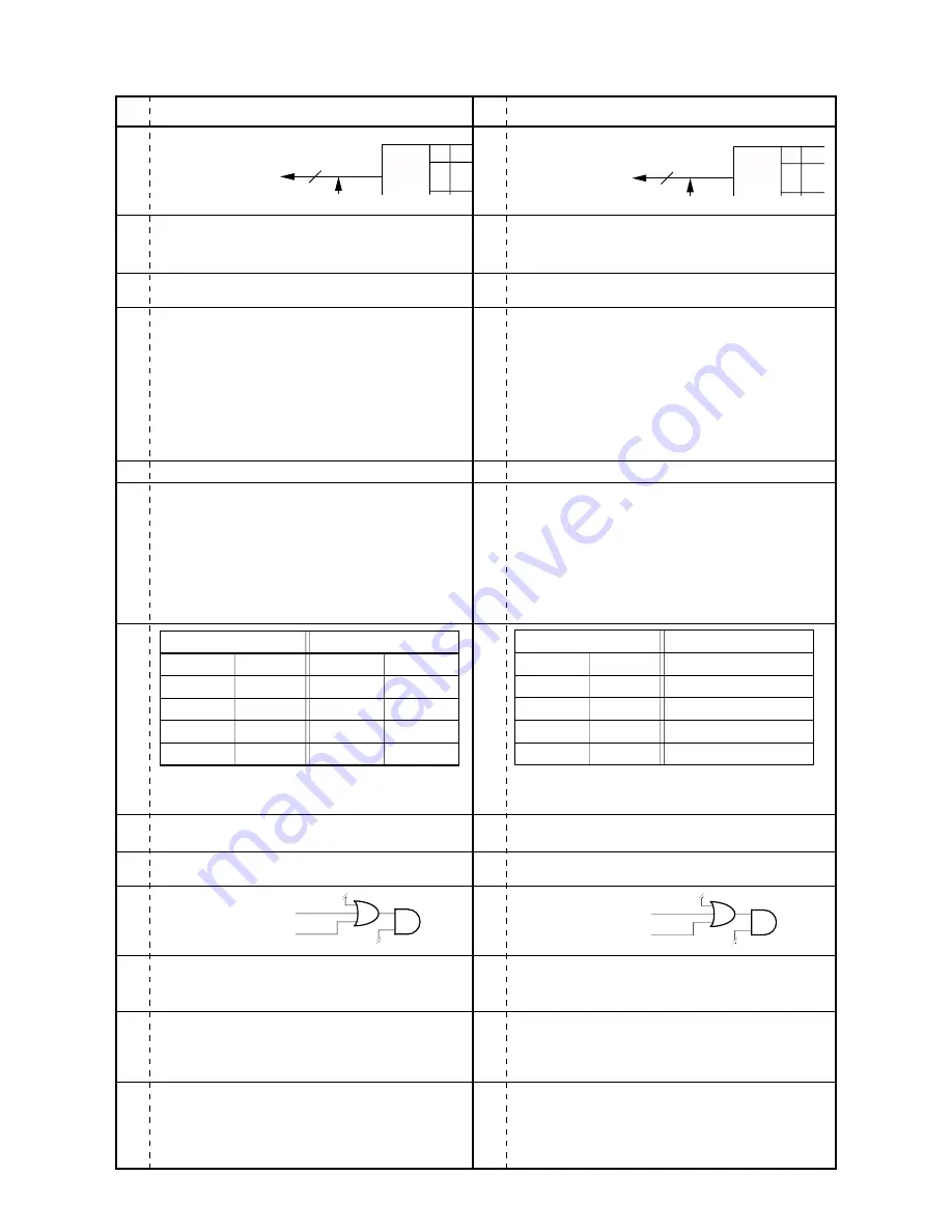
(In fig. 9-4-1.)
(Register's purpose)
This register determines whether an NMI interrupt has been generated.
Bit name
Description
NMIF
External NMI request flag
(From 1st line of main sentence)
Each flag is set if the corresponding NMI interrupt request is
generated.
After an NMI interrupt is accepted, clear it via the software from
within the NMI interrupt processing program.
When a flag is set to “1”, write a “1” to the flag to clear it.
Note: An NMI cannot be generated through software.
(The 3rd line right after the itemizations.)
..., it is determined to be either a non-maskable interrupt (NMI) ...
(The 2nd line from the bottom.)
..., the NMI interrupt request is simply sent to the CPU.
When the CKSEL pin input is "H" (oscillating frequency: 8 to 15 MHz):
16, 18, 20, 22, or 24 bits can be selected.
When the CKSEL pin input is "L" (oscillating frequency: 8 to 30 MHz):
Overflow cycle: 4.369 ms to 1118.481 ms
(when the CKSEL pin input is "H" and the oscillating frequency is 15 MHz)
4.369 ms to 1118.481 ms
(when the CKSEL pin input is "L" and the oscillating frequency is 30 MHz)
(The 2nd line from the bottom.)
When recovering from STOP mode: 4.369 ms to 1118.481 ms
(In fig. 9-4-1.)
(Register's purpose)
This register determines whether a non-maskable interrupt has been
generated.
Bit name
Description
NMIF
External non-maskable interrupt request flag
(From 1st line of main sentence)
The method of clearing flag differs according to the interrupt request
flags.
1. External non-maskable interrupt request flag (NMIF) and Watchdog
timer overflow interrupt request flag (WDIF)
After a non-maskable interrupt is accepted, these flags can be cleared
by writing to the non-maskable interrupt control register (NMICR).
When a flag is set to “1”, write a “1” to the flag to clear it.
Note: A non-maskable interrupt cannot be generated through software.
(Following sentence is added to under the table shown the change of flag.)
2. System error interrupt request flag (SYSEF)
This flag cannot be cleared by writing to the non-maskable interrupt
control register (NMICR).
This flag can be cleared by generating a reset interrupt by setting the
_______
RST pin to "L" level or by the self-reset, which is generated by writing
to the reset control register (RSTCTR) of the watchdog timer.
(The 3rd line right after the itemizations.)
..., it is determined to be either a non-maskable interrupt ...
(The 2nd line from the bottom.)
..., the non-maskable interrupt request is simply sent to the CPU.
When the CKSEL pin input is "H" (oscillating frequency: 8 MHz to 18 MHz):
16, 18, 20, 22, or 24 bits can be selected.
When the CKSEL pin input is "L" (oscillating frequency: 8 MHz to 20 MHz):
Overflow cycle: 4.369 ms to 1118.481 ms
(when the CKSEL pin input is "H" and the oscillating frequency is 15 MHz)
(The 2nd line from the bottom.)
When recovering from STOP mode: 4.369 ms to 1118.481 ms
<Recommended value is 14 ms or longer.>
P.9-3
P.9-7
P.9-7
P.9-7
P.9-7
P.9-7
P.9-8
P.9-30
P.9-30
P.11-6
P.12-2
P.12-2
P.12-2
Non-maskable
interrupts
GROUP
0
1
0
NMI
GROUP
0
1
0
Note) n= 0, 1, 2, 3
IRn
0
1
0
1
IDn
0
0
1
1
IRn
No change
No change
0
1
IDn
No change
No change
0
IEn value
Write data
Result of write
Note) n= 0, 1, 2, 3
The value of IDn after the write is the logical product of the value of IEn
after the write and the value of IRn after the write.
IRn
0
1
0
1
IDn
0
0
1
1
IRn
No change
No change
0
1
Write data
Result of write
Single-buffer mode
Initialization flag (TM6LDE)
Single-buffer mode
Initialization flag (TM10LDE)
Summary of Contents for MN103001G/F01K
Page 1: ...MICROCOMPUTER MN1030 MN103001G F01K LSI User s Manual Pub No 23101 050E ...
Page 2: ......
Page 4: ......
Page 6: ......
Page 8: ......
Page 9: ...Table of Contents List of Figures and Tables 0 ...
Page 26: ...xviii ...
Page 27: ...1 0 1 General Specifications ...
Page 35: ...2 CPU 2 ...
Page 57: ...3 Extension Instruction Specifications 3 ...
Page 96: ...Extension Instruction Specifications 3 40 ...
Page 97: ...4 Memory Modes 3 4 ...
Page 102: ...Memory Modes 4 6 ...
Page 103: ...5 Operating Mode 5 ...
Page 107: ...6 Clock Generator 6 13 ...
Page 111: ...7 Internal Memory 7 ...
Page 114: ...Internal Memory 7 4 ...
Page 115: ...8 Bus Controller BC 8 ...
Page 189: ...9 Interrupt Controller 9 ...
Page 220: ...Interrupt Controller 9 32 ...
Page 221: ...10 8 bit Timers 9 10 ...
Page 254: ...8 bit Timers 10 34 ...
Page 255: ...11 16 bit Timers 11 ...
Page 292: ...16 bit Timers 11 38 ...
Page 293: ...12 Watchdog Timer 11 12 ...
Page 302: ...Watchdog Timer 12 10 ...
Page 303: ...13 Serial Interface 13 ...
Page 354: ...Serial Interface 13 52 ...
Page 355: ...14 A D Converter 14 ...
Page 367: ...15 I O Ports 15 ...
Page 431: ...16 Internal Flash Memory 16 ...
Page 439: ...17 17 Ordering Mask ROM ...
Page 442: ...Ordering Mask ROM 17 4 ...
Page 443: ...Appendix ...


