


MOTOROLA
MC68306 USER'S MANUAL
3- 17
The bus request from the granted device should be negated after
BGACK
is asserted. If
another bus request is pending,
BG
is reasserted within a few clocks, as described in 3.3
Bus Arbitration Control. The processor does not perform any external bus cycles before
reasserting
BG
.
3.3 BUS ARBITRATION CONTROL
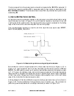
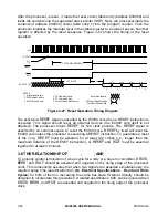
All asynchronous bus arbitration signals to the processor are synchronized before being
used internally. As shown in Figure 3-16, synchronization requires a maximum of one and
a half cycles of the system clock. The input asynchronous signal is sampled on the falling
edge of the clock and is valid internally after the next rising edge.
This synchronization scheme is used for all other asynchronous inputs also:
RESET,
HALT, DTACK, BERR, IPL2–IPL0
.
CLK
BR (EXTERNAL)
BR (iNTERNAL)
47
INTERNAL SIGNAL VALID
EXTERNAL SIGNAL SAMPLED
Figure 3-16. External Asynchronous Signal Synchronization
Bus arbitration control is implemented with a finite state machine (see Figure 3-17). In
Figure 3-17, input signals R and A are the internally synchronized versions of
BR
and
BGACK
. The
BG
output is shown as G, and the internal three-state control signal is shown
as T. If T is true, the address, data, and control buses are placed in the high-impedance
state when
AS
is negated. All signals are shown in positive logic (active high), regardless
of their true active voltage level. State changes (valid outputs) occur on the next rising
edge of the clock after the internal signal is valid.
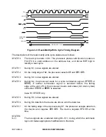
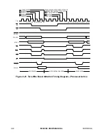
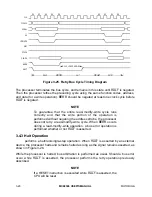
A timing diagram of the bus arbitration sequence during a processor bus cycle is shown in
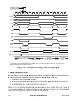
Figure 3-18. The bus arbitration timing while the bus is inactive (e.g., the processor is
performing internal operations for a multiply instruction) is shown in Figure 3-19.