


MOTOROLA
MC68306 USER'S MANUAL
8- 9
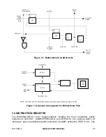
8.8 AC ELECTRICAL SPECIFICATIONS—CHIP SELECTS AND
INTERRUPT ACKNOWLEDGE
(The electrical specifications in this document are preliminary.)
16.67 MHz
Num
Characteristic
Min
Max
Unit
61
Address Valid to
CS≈
Asserted (Read or Write)
15
—
ns
61A
FC Valid to
CS≈
Asserted (Read or Write)
45
—
ns
62
AS
V
DS
to
CS≈
0
5
ns
63
AS
V R/
W
to
CS≈
0
5
ns
64
CS≈
Width Asserted
120
—
ns
65
CS≈
Negated to FC, Addess Invalid
15
—
ns
66
CS≈
Negated to R/
W
Invalid
15
—
ns
67
Data-Out Valid to
CS≈
Negated (Write)
90
—
ns
68
CS≈
Negated to Data-Out Invalid (Write)
15
—
ns
69
CS≈
Negated to Data-In High Impedance
—
90
ns
70
CLKOUT High to
IACK≈
Asserted
0
30
ns
70A
LDS
High to
IACK≈
Negated
0
10
ns
V = Boolean OR
S0
S1
S2
S3
S4
S5
S6
CLKOUT
FC2–FC0,
A23–A0
AS
R/W
DATA
(NOTE 1)
LDS / UDS
CS
S12
S13
S14
S15
S16
S17
S18
62
62
63
65
65
66
63
67
68
READ
WRITE
(NOTE 1)
9A
9A
OE
UW, LW
NOTE: THE WRITE CYCLE ILLUSTRATED IS PART OF A TEST AND SET INSTRUCTION.
61
61
64
69
IN
OUT
64
IACKx
70
61A
70A
12A
61A
12A
Figure 8-5. Chip Select and Interrupt Acknowledge Timing Diagram