


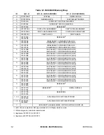


5- 12
MC68306 USER'S MANUAL
MOTOROLA
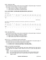
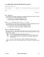
Figure 5-1 shows a method of expanding the number of chip selects in case more are
required for the application.
MC68306
74F138
ADDR
CS7
A0
A1
A2
E1
E3
E2
Q0
Q1
Q2
Q3
Q4
Q5
Q6
Q7
EXCS0 ($080XXX)
EXCS1 ($088XXX)
EXCS2 ($090XXX)
EXCS3 ($098XXX)
EXCS4 ($0A0XXX)
EXCS5 ($0A8XXX)
EXCS6 ($0B0XXX)
EXCS7 ($0B8XXX)
A15
A16
A17
A18
A19
CS0
CS1
CS2
CS3
CS4
CS5
CS6
AMODE
}
}
1 MBYTE ADDRESS
SPACE EACH
32 KBYTE ADDRESS
SPACE EACH
1
2
3
4
5
6
Figure 5-1. Chip Select Expansion
5.2.7 DRAM Control Registers
The DRAM address space decode mechanism is identical to the chip select mechanism.
Bank 0 has priority over bank 1, but all chip selects have priority over DRAM. The
MC68306 DRAM controller provides CAS-before-RAS refresh only. The refresh timer is a
programmable period counter that generates a refresh request every 16 to 4096 EXTAL
periods, programmable in 16 EXTAL period increments. Programming the refresh rate is
described in paragraph 5.2.7.1. When a refresh is pending, a refresh cycle is inserted at
the earliest availability of the RAS/CAS signals. Both banks and both bytes are refreshed
together.
The refresh timer is not affected by any reset, and refresh cycles will appear under reset.
The refresh timer is initialized by a write to the refresh rate register. When this register is
written, the first refresh occurs immediately, so the refresh rate should be programmed
after the DRAM configuration register DRDT bit. After power-up, the refresh rate register
value is random. If power consumption is critical, the refresh rate should be set as soon as
possible. In a system with soft-reset recovery, the hard/soft reset decision could take a
long time. A safe algorithm is to read the register first; if it contains the correct value, do
nothing. This will not disturb the timer, and the reset recovery can proceed at leisure.
Refresh stops only when the MC68306 is arbitrated off the bus. If the internal EC000
BG
signal is asserted while a refresh cycle is in progress, the external
BG
signal is delayed
until the refresh is complete. However, no refresh will occur during another master's
tenure of the bus if the
BG
or
BGACK
signals are recognized before a refresh cycle starts.
The task of DRAM refresh must be assumed by any other bus master. The refresh timer is
not suspended while the bus is arbitrated away, so a refresh cycle is likely when the