


3- 10
MC68306 USER'S MANUAL
MOTOROLA
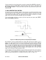
STATE 12
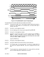
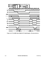
The write portion of the cycle starts in S12. The valid function codes on
FC2–FC0, the address bus lines,
AS
, and R/
W
remain unaltered.
STATE 13
During S13, no bus signals are altered.
STATE 14
On the rising edge of S14, the processor drives R/
W
low.
STATE 15
During S15, the data bus is driven out of the high-impedance state as the
data to be written are placed on the bus.
STATE 16
At the rising edge of S16, the processor asserts
UDS
/
LDS
. The processor
waits for
D T A C K
or
BERR
. If neither termination signal is asserted
before the falling edge at the close of S16, the processor inserts wait states
(full clock cycles) until either
DTACK
or
BERR
is asserted.
Case W1:
DTACK
with or without
BERR
.
STATE 17
During S17, no bus signals are altered.
STATE 18
During S18, no bus signals are altered.
STATE 19
On the falling edge of the clock entering S19, the processor negates
AS
and
UDS
/
LDS
. As the clock rises at the end of S19, the processor
places the data bus in the high-impedance state, and drives
R/
W
high. The device negates
DTACK
or
BERR
at this time.
Case R2:
DTACK
and
BERR
on read.
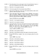
STATE 5
During S5, no bus signals are altered.
STATE 6
During S6, no bus signals are altered, and data from the device is ignored.
STATE 7
AS
and
U D S
/
LDS
are negated. The cycle terminates without the write
portion.
Case R3:
BERR
only on read.
STATE 5
During S5, no bus signals are altered.
STATE 6
During S6, no bus signals are altered..
STATE 7
During S7, no bus signals are altered.
STATE 8
During S8, no bus signals are altered.
STATE 9
AS
and
U D S
/
LDS
are negated. The cycle terminates without the write
portion.
Case W2:
BERR
only on write.