


7- 4
MC68306 USER'S MANUAL
MOTOROLA
The XTAL and X2 pins are associated with analog signals and are not included in the
boundary scan register.
All MC68306 bidirectional pins, except the open-drain I/O pins (
HALT, DTACK,
BERR,
and
RESET
), have a single register bit for pin data and an associated control bit in the
boundary scan register. All open drain I/O pins have a single register bit for pin data and
no associated control bit. To ensure proper operation, the open-drain pins require external
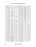
pullups. Twenty-four control bits in the boundary scan register define the output enable
signal for associated groups of bidirectional and three-state pins. The control bits and their
bit positions are listed in Table 7-1.
Table 7-1. Boundary Scan Control Bits
Name
Bit Number
Name
Bit Number
Name
Bit Number
OPOE3
8
PPOE15
26
PPOE7
42
PPOE8
12
PPOE0
28
DOE
58
PPOE9
14
PPOE1
30
HiZ
67
PPOE10
16
PPOE2
32
DRAMWOE
86
PPOE11
18
PPOE3
34
DRAMOE
88
PPOE12
20
PPOE4
36
CPMOE
97
PPOE13
22
PPOE5
38
CSOE
100
PPOE14
24
PPOE6
40
AOE
118
Boundary scan bit definitions are shown in Table 7-2. The first column in Table 7-2 defines
the bit's ordinal position in the boundary scan register. The shift register bit nearest TDO
(i.e., first to be shifted out) is defined as bit 0; the last bit to be shifted out is bit 123.
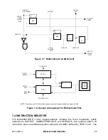
The second column references one of the five MC68306 cell types depicted in Figures
7-3–7-7, which describe the cell structure for each type.
The third column lists the pin name for all pin-related bits or defines the name of
bidirectional control register bits.
The last column indicates the associated boundary scan register control bit.
Bidirectional pins include a single scan bit for data (IO.Cell) as depicted in Figure 7-7.
These bits are controlled by one of the two bits shown in Figures 7-5 and 7-6. The value of
the control bit determines whether the bidirectional pin is an input or an output. One or
more bidirectional data bits can be serially connected to a control bit as shown in Figure
7-8. Note that, when sampling the bidirectional data bits, the bit data can be interpreted
only after examining the IO control bit to determine pin direction.