


MOTOROLA
MC68306 USER'S MANUAL
6-5
.. .
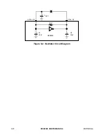
ADDRESS BUS
I
N
T
E
R
N
A
L
B
U
S
DATA
D7–D0
EXTERNAL
INTERFACE SIGNALS
X1/CLK
X2
BAUD RATE
GENERATOR
LOGIC
CHANNEL B
FOUR-CHARACTER
RECEIVE BUFFER
TWO-CHARACTER
TRANSMIT BUFFER
RxDB
TxDB
CHANNEL A
FOUR-CHARACTER
RECEIVE BUFFER
TWO-CHARACTER
TRANSMIT BUFFER
RxDA
TxDA
CONTROL
INTERNAL
CONTROL
LOGIC
S
E
R
I
A
L
M
O
D
U
L
E
INTERFACE
TO CPU
INPUT PORT
OUTPUT PORT
IRQ
TIRQ
16-BIT
COUNTER/TIMER
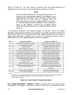
Figure 6-2. External and Internal Interface Signals
6.2.4 Channel A Receiver Serial Data Input (RxDA)
This signal is the receiver serial data input for channel A. Data received on this signal is
sampled on the rising edge of the clock source, with the least significant bit received first.
6.2.5 Channel B Transmitter Serial Data Output (TxDB)
This signal is the transmitter serial data output for channel B. The output is held high
('mark' condition) when the transmitter is disabled, idle, or operating in the local loopback
mode. Data is shifted out on this signal at the falling edge of the clock source, with the
least significant bit transmitted first.