


3- 4
MC68306 USER'S MANUAL
MOTOROLA
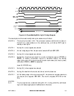
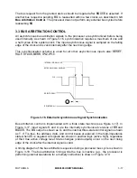
A bus cycle consists of eight states. The various signals are asserted during specific
states of a read cycle as follows:
STATE 0
The read cycle starts in state 0 (S0). The processor places valid function
codes on FC0–FC2, a valid address on the bus, and drives R/
W
high to
identify a read cycle.
STATE 1
During state 1 (S1), no bus signals are altered.
STATE 2
On the rising edge of state 2 (S2), the processor asserts
AS
and
UDS/LDS
.
STATE 3
During state 3 (S3), no bus signals are altered.
STATE 4
During state 4 (S4), the processor waits for a cycle termination signal
(
DTACK
or
BERR
). If neither termination signal is asserted before the falling
edge at the end of S4, the processor inserts wait states (full clock cycles)
until either
DTACK
or
BERR
is asserted.
Case 1:
DTACK
received, with or without
BERR
.
STATE 5
During state 5 (S5), no bus signals are altered.
STATE 6
Sometime between state 2 (S2) and state 6 (S6), data from the device is
driven onto the data bus.
STATE 7
On the falling edge of the clock entering state 7 (S7), the processor latches
data from the addressed device and negates
AS
and
UDS
,
LDS
. The device
negates
DTACK
or
BERR
at this time.
Case 2:
BERR
received without
DTACK
.
STATE 5
During state 5 (S5), no bus signals are altered.
STATE 6
During state 6 (S6), no bus signals are altered.
STATE 7
During state 7 (S7), no bus signals are altered.
STATE 8
During state 8 (S8), no bus signals are altered.
STATE 9
AS
and
UDS/LDS
negated. Slave negates
BERR.
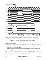
3.1.2 Write Cycle
During a write cycle, the processor sends bytes of data to the memory or peripheral
device. If the instruction specifies a word or long-word operation, the processor issues
both
UDS
and
LDS
and writes both bytes. A long-word write is accomplished by two
consecutive word writes. When the instruction specifies a byte operation, the processor
uses the internal A0 bit to determine which byte to write and issues the appropriate data