background image

MDDR Subsystem

Microsemi Proprietary UG0446 User Guide Revision 7.0

50

3.6.4

Accessing MDDR from the HPDMA

The HPDMA controller can access DDR SDRAM connected to the MDDR subsystem through the HPMS 
DDR bridge. The following illustration shows the MDDR with HPDMA.

Figure 29 • 

MDDR with HPDMA

The following steps describe how to access the MDDR from HPDMA:

1.

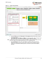
Open the 

System Builder - Device Features

 tab. Check the 

HPMS External DDR Memory 

check 

box, select 

MDDR

 and 

HPMS High Performance DMA (HPDMA) 

check boxes, leaving the rest of 

the check boxes unchecked. The following image shows the 

System Builder - Device Features


tab.

Figure 30 • 

System Builder - Device Features Tab

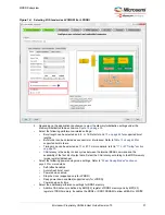
2.

Configure the 

HPMS External Memory in Memories

 tab. as shown in the following image. In this 

example, the design is created to access the DDR3 memory with a 32-bit data width and no ECC.

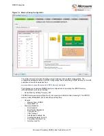
3.

Set the

 DDR memory settling time

 to 200 us and click 

Import Register Configuration

.

FIC_0

FIC_1

AHB Bus Matrix

D
D
R

I

O

 Fabric

HPMS DDR 

Bridge

IGLOO2

DDR 

Controller

D
D

P

H

Y

APB Config 

Reg

MDDR

AXI 

Transaction 

Controller

HPDMA

HPMS

DDR 

SDRAM

AHB  

CoreConfigMaster

APB_2

CoreConfigP

eNVM

eSRAM

Summary of Contents for Microsemi IGLOO2

Page 1: ...UG0446 User Guide SmartFusion2 and IGLOO2 FPGA High Speed DDR Interfaces...

Page 2: ...i It is the Buyer s responsibility to independently determine suitability of any products and to test and verify the same The information provided by Microsemi hereunder is provided as is where is and...

Page 3: ...ing MDDR from the HPDMA 50 3 7 Timing Diagrams 52 3 8 Timing Optimization Technique for AXI 55 3 9 DDR Memory Device Examples 58 3 9 1 Example 1 Connecting 32 Bit DDR2 to MDDR_PADs 58 3 9 2 Example 2...

Page 4: ...to FDDR_PADs 173 4 8 2 Example 2 Connecting 32 Bit DDR3 to FDDR_PADs with SECDED 173 4 8 3 Example 3 Connecting 16 Bit LPDDR to FDDR_PADs with SECDED 174 4 9 FDDR Configuration Registers 175 4 9 1 FD...

Page 5: ...oller Fabric Interface Controller 219 6 1 Functional Description 220 6 1 1 Port List 220 6 2 How to Use SMC_FIC in IGLOO2 Device 225 6 3 SYSREG Control Register for SMC_FIC 227 6 4 Appendix A How to U...

Page 6: ...Design Connections Top Level View 48 Figure 28 MDDR with Single AHB Lite Interface 49 Figure 29 MDDR with HPDMA 50 Figure 30 System Builder Device Features Tab 50 Figure 31 Memory Configurations 51 Fi...

Page 7: ...Figure 83 Fabric DDR Memory Configuration 160 Figure 84 Selecting I O Standard as LVCMOS18 or LPDDRI 161 Figure 85 Memory Initialization Configuration 163 Figure 86 Memory Timing Configuration 164 Fi...

Page 8: ...gure 128 DDR Bridge Functional Block Diagram 209 Figure 129 WCB Operation 210 Figure 130 Flow Chart for Read Operation 211 Figure 131 System Builder Device Features Window 213 Figure 132 Configuring H...

Page 9: ...ble 22 DDR I O Standard is Configured Based on I O Drive Strength Setting 35 Table 23 MDDR Throughput for AHB 49 Table 24 Number of Cycles for AXI AHB Transactions to MDDR 55 Table 25 I O Standards an...

Page 10: ...TUS_SR 91 Table 81 DDRC_LUE_SYNDROME_1_SR 92 Table 82 DDRC_LUE_SYNDROME_2_SR 92 Table 83 DDRC_LUE_SYNDROME_3_SR 93 Table 84 DDRC_LUE_SYNDROME_4_SR 94 Table 85 DDRC_LUE_SYNDROME_5_SR 94 Table 86 DDRC_L...

Page 11: ...ced Bank Constraints 154 Table 138 Dynamic DRAM Global Constraints 154 Table 139 Supported Address Width Range for Row Bank and Column 159 Table 140 DDR I O Standard is Configured based on I O Drive S...

Page 12: ...le 94 page 99 SAR 75057 Updated Architecture Overview page 136 SAR 79005 Added DDR Memory Initialization Time page 18 SAR 72725 Updated Appendix B Register Lock Bits Configuration page 204 SAR 79864 1...

Page 13: ...Interface Controller page 219 SAR 54036 Updated MDDR Memory Map page 30 SAR 44198 Updated Address Mapping page 155 SAR 45761 1 7 Revision 1 0 The following is a summary of the changes in this revision...

Page 14: ...tics DS0124 IGLOO2 Pin Descriptions Datasheet This document contains IGLOO2 pin descriptions package outline drawings and links to pin tables in Excel format DS0115 SmartFusion2 Pin Descriptions Datas...

Page 15: ...ially all the security features that made third generation Microsemi SoC devices the gold standard for security in the PLD industry Also included are unique design and data security features and use m...

Page 16: ...3 33 MHz DDR performance Supports memory densities upto 4GB Supports 8 16 32 bit DDR standard dynamic random access memory SDRAM data bus width modes Supports a maximum of 8 memory banks Supports sing...

Page 17: ...udes length matching and follows AC393 SmartFusion2 and IGLOO2 Board Design Guidelines Application Note For Read Leveling Libero SOC auto generates pre defined static delay ratios for MDDR initializat...

Page 18: ...upported Memory DDR2 DDR3 and LPDDR1 Configurations Memory Depth Width Width in SECDED Mode SmartFusion2 and IGLOO2 Devices M2S M2GL 005 010 025 060 090 M2S M2GL150 FCV484 M2S M2GL 050 FCS325 VF400 FG...

Page 19: ...troller receives read and write requests from AXI masters MSS HPMS DDR bridge and DDR_FIC and schedules for the DDR controller by translating them into DDR controller commands The DDR controller recei...

Page 20: ...nel sideband signal and is valid with the AWVALID signal HPMS_DDR_FIC_SUBSYSTEM_CLK or MSS_DDR_FIC_SUBSYSTEM_CLK Out This output clock is derived from the MDDR_CLK and is based on the DDR_FIC divider...

Page 21: ...out DRAM data input output for bidirectional pads MDDR_DQ_ECC 3 0 In out DRAM data input output for SECDED MDDR_DM_RDQS_ECC In out High DRAM single ended data strobe output for bidirectional pads MDD...

Page 22: ...R_AXI_S_BRESP 1 0 Output Indicates write response This signal indicates the status of the write transaction 00 Normal access okay 01 Exclusive access okay 10 Slave error 11 Decode error MDDR_DDR_AXI_S...

Page 23: ...ary 11 Reserved MDDR_DDR_AXI_S_ARID 3 0 Input Indicates identification tag for the read address group of signals MDDR_DDR_AXI_S_ARLEN 3 0 Input Indicates burst length The burst length gives the exact...

Page 24: ...orted 01 INCR Incrementing address burst normal sequential memory 10 WRAP Incrementing address burst that wraps to a lower address at the wrap boundary 11 Reserved MDDR_DDR_AXI_S_AWID 3 0 Input Indica...

Page 25: ...read data and response information 1 Master ready 0 Master not ready MDDR_DDR_AXI_S_WDATA 63 0 Input Indicates write data MDDR_DDR_AXI_S_WID 3 0 Input Indicates response ID The identification tag of t...

Page 26: ...BUSY 10 NONSEQUENTIAL 11 SEQUENTIAL MDDR_DDR_AHBx_S_HMASTLOCK Input High Indicates AHB master lock signal from Fabric master MDDR_DDR_AHBx_S_HWRITE Input High Indicates AHB write control signal from F...

Page 27: ...Calibration Each DDRIO has an ODT feature which is calibrated depending on the DDR I O standard DDR I O calibration occurs after the DDR I Os are enabled If the impedance feature is enabled impedance...

Page 28: ...is met before ZQCL or ZQCS commands are issued by the DDR controller 3 5 3 4 DRAM Training High Speed DDR3 memories typically requires the DDR controller to implement Write Leveling Read DQS Gate Trai...

Page 29: ...IGLOO2 Board Design Guidelines refer AC393 Board Design Guidelines for SmartFusion2 IGLOO2 FPGA Application Note Note The Libero SOC auto generated delay ratio for read DQS data eye centering is writ...

Page 30: ...nd FDDR chapter on page 216 for a detailed description The DDR_FIC input interface is clocked by the FPGA fabric clock and the MDDR is clocked by MDDR_CLK from the MSS HPMS CCC Clock ratios between MD...

Page 31: ...es the handshaking signals on the AXI interface 3 5 4 2 2 Priority Block The priority block prioritizes AXI read write transactions and provides control to the transaction handler AXI read transaction...

Page 32: ...ntroller receives requests from the AXI transaction controller performs the address mapping from system addresses to DRAM addresses rank bank row and column and prioritizes requests to minimize the la...

Page 33: ...des with the queued write the DDR controller overwrites the data for the queued write with that from the new write and only performs one write transaction The write combine functionality can be disabl...

Page 34: ...width and burst length 8 Figure 8 DDR RMW Operation 16 Bit DDR Bus Width and Burst Length 8 The following illustration shows the DDR controller burst transactions to DRAM for unaligned 64 bit AXI writ...

Page 35: ...d DDRC_LUE_ADDRESS_2_SR give the row bank column information of the SECDED unrecoverable error 2 DDRC_LCE_ADDRESS_1_SR and DDRC_LCE_ADDRESS_2_SR give the row bank column information of the SECDED erro...

Page 36: ...ializes DDR memories through an initialization sequence depending on the type of DDR memory used For more information on the initialization process refer to the JEDEC specification 3 5 5 MDDR Subsyste...

Page 37: ...ble 13 Supported Burst Modes Bus Width Memory Type Sequential Interleaving 4 8 32 LPDDR1 DDR2 DDR3 16 LPDDR1 DDR2 DDR3 8 LPDDR1 DDR3 DDR2 Table 14 Dynamically Enforced Bank Constraints Timing Constrai...

Page 38: ...the programmed value for that register as described in EQ 1 Table 15 Dynamically Enforced Bank Constraints Timing Constraints of DDR Memory Control Bit Description Nominal refresh cycle time tRFC nom...

Page 39: ...ing registers DDRC_ADDR_MAP_BANK_CR DDRC_ADDR_MAP_COL_1_CR DDRC_ADDR_MAP_COL_2_CR DDRC_ADDR_MAP_COL_3_CR DDRC_ADDR_MAP_ROW_1_CR DDRC_ADDR_MAP_ROW_2_CR While configuring the registers ensure that two D...

Page 40: ...memory visible in the other memory space is mirrored of this 512 MB memory 3 5 5 7 DDR Mode Registers After reset the DDR controller initializes the mode registers of DDR memory with the values in th...

Page 41: ...ency of the bus to one command per two clocks but it doubles the amount of setup and hold time The data bus remains the same for all of the variations in the address bus and the default configuration...

Page 42: ...sed on Mode Settings for 4 GB Memory Address Space Mapping Modes DDR Memory Regions Visible at MSS HPMS DDR Address Space for Different Modes MSS HPMS DDR Space 0 0 A0000000 0 AFFFFFFF MSS HPMS DDR Sp...

Page 43: ...Peripheral Initialization User Guide Table 19 Accessed DDR Memory Regions Based on Mode Settings for a 2 GB Memory Address Space Mapping Modes DDR Memory Regions Visible at MSS HPMS DDR Address Space...

Page 44: ...7 0 33 Figure 11 System Builder Device Features Window For more information about how to use MDDR in the SmartFusion2 devices refer to Appendix A How to Use the MDDR in SmartFusion2 section on page 11...

Page 45: ...B Master accesses the DDR configuration data stored in eNVM through FIC_0 The configuration data is sent to CoreConfigIP through the FIC_2 master port CoreConfigP sends the configuration data to APB b...

Page 46: ...ing section Select the I O Drive Strength as Half Drive Strength or Full Drive Strength as shown in Figure 13 page 36 The following table lists how the DDR I O standard is configured based on this set...

Page 47: ...I SSTL18 because the board is designed to use the LPDDRI I O standard Note If LVCMOS18 is selected all I Os are configured to LVCMOS1 8 except CLK CLK_N CLK and CLK_N which are configured to the LPDDR...

Page 48: ...T For more details refer to 1T or 2T Timing section on page 30 CAS latency is the delay in clock cycles between the internal READ command and the availability of the first bit of output data Select th...

Page 49: ...n options of RZQ 6 and RZQ 7 The partial array self refresh coverage setting is defined by EMR 2 0 register bits of LPDDR memory with drop down options of Full Quarter One eighth and One sixteenth Thi...

Page 50: ...Figure 15 Memory Initialization Configuration 6 Select the memory timing settings under the Memory Timing tab according to the DDR memory vendor datasheet as shown in the following image For more det...

Page 51: ...documents LPDDR_Emcraft_Config zip The following is an example of MDDR register configurations for operating the LPDDR memory MT46H64M16LF with clock 166 MHz Device Memory Settling Time s 200 The DDR...

Page 52: ...for the design Drag and drop the required master slave to the corresponding subsystem The following image shows the Peripherals tab Drag and drop the Fabric Master core to the HPMS DDR FIC Subsystem...

Page 53: ...s intended to run DDR_FIC_CLK can be configured as a ratio of MDDR_CLK 1 2 3 4 6 8 12 16 or 32 using the Clocks configurator The maximum frequency of DDR_FIC_CLK is 200 MHz The following illustration...

Page 54: ...FPGA Fabric through the AXI Interface The AXI master in the FPGA fabric accesses the DDR memory through the MDDR subsystem The following illustration shows the MDDR subsystem with the AXI interface T...

Page 55: ...write the data to the DDR memory after initializing the MDDR registers The following steps describe how to access the MDDR from AXI master in the FPGA fabric FIC_0 FIC_1 AHB Bus Matrix D D R I O Fabr...

Page 56: ...ation In this example the design is created to access DDR3 memory with a 32 bit data width and no ECC 3 Set the DDR memory settling time to 200 us and click Import Register Configuration Figure 23 Mem...

Page 57: ...and then click OK The following image shows the AMBA Master Configuration dialog Figure 25 AMBA Master Configuration 8 Configure the System Clock and Subsystem clocks in the Clocks tab The following...

Page 58: ...canvas to access the MDDR subsystem through the AXI interface Ensure that the AXI master logic accesses the MDDR after configuring the MDDR registers INIT_DONE indicates the successful MDDR initializa...

Page 59: ...I throughput see AC422 SmartFusion2 Optimizing DDR Controller for Improved Efficiency Libero v11 7 Application Note 3 6 3 Accessing MDDR from FPGA Fabric Through the AHB Interface The MDDR subsystem c...

Page 60: ...DR Mode DDR3 Fabric Clock to MDDR Clock Ratio 1 4 PHY Width 16 and 32 Clock Frequency 80 MHz The other parameters are configured similar to the MDDR configuration in AC422 SmartFusion2 Optimizing DDR...

Page 61: ...rformance DMA HPDMA check boxes leaving the rest of the check boxes unchecked The following image shows the System Builder Device Features tab Figure 30 System Builder Device Features Tab 2 Configure...

Page 62: ...g Select the On chip 25 50 MHz RC Oscillator Configure HPMS_CCC for MDDR_CLK 5 Configure HPMS_CLK APB_0_CLK FIC_0_CLK clocks as 111 MHz and the MDDR_CLK clock as 333 MHz Figure 32 Clocks Configuration...

Page 63: ...DDR_CS_N MDDR_ODT MDDR_RAS_N MDDR_RESET_N MDDR_WE_N MDDR_ADDR MDDR_BA MDDR_DM_RDQS MDDR_DQS MDDR_DQS_N MDDR_DQ MDDR_DQS_TMATCH_0_IN MDDR_DQS_TMATCH_0_OUT CLK AWID AWADDR AWLEN AWSIZE AWLOCK AWBURST AW...

Page 64: ...n Read transac on to DDR Memory ini ated by MDDR 0 2 3 4 1 6 7 8 5 10 11 12 9 14 15 16 13 18 19 20 17 22 23 24 21 26 27 28 25 30 31 32 33 29 55 54 0000 0 0008 0 0010 0018 0020 0028 0038 0030 56 58 59...

Page 65: ..._0_out 0 0 0 0 0 0 0 0 0 0 0 0 0 0 0 0 0 0 0 0 0 0 0 0 0 0 0 0 0 0 0 0 0 0 0 0 0 0 0 0 0 0 0 0 0 0 0 0 0 0 0 0 0 0 0 0 0 0 0 0 0 0 0 0 0 0 0 0 0 3 1 2 3 4 5 6 7 8 9 10 11 12 13 14 15 16 3 3 3 3 3 3 3...

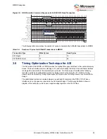
Page 66: ...1 interface Timing closure can be achieved by Timing Optimization Technique when the timing closure is not met with the design The optimization method can reside between an existing AXI master and the...

Page 67: ...e timing SDC file It applies the proper timing relaxation on the DDR_FIC_AXI signals For FDDR The following constraints provide a relaxation constraint on the signals of 1 5 clock periods The user sho...

Page 68: ..._AXI INST_FDDR_IP F_RREADY The following constraints provide a relaxation constraint on the signals of 1 clock period set delay2 expr 2000 ddr_clock_frequency set_max_delay delay2 to get_pins INST_FDD...

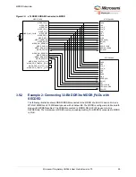
Page 69: ..._clock_frequency set_max_delay delay2 to get_pins INST_MSS_ _IP F_ARVALID INST_MSS_ _IP F_AWVALID INST_MSS_ _IP F_WVALID 3 9 DDR Memory Device Examples This section describes how to connect DDR memori...

Page 70: ...ed to store SECDED bits The total amount of DDR3 memory excluding memory for SECDED connected to MDDR is 2 GB CASN CKE CLK_P CLK_N CSN ODT RASN WEN ADDR 12 0 BA 2 0 MT47H64M16 MDDR_CAS_N MDDR_CKE MDDR...

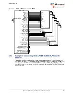
Page 71: ...LK_P CLK_N CSN ODT RASN RSTN WEN ADDR 15 0 BA 2 0 MT41J512M8RA MDDR_CAS_N MDDR_CKE MDDR_CLK MDDR_CLK_N MDDR_CS_N MDDR_ODT MDDR_RAS_N MDDR_RESET_N MDDR_WE_N MDDR_ADDR 15 0 MDDR_BA 2 0 MDDR_DM_RDQS 0 MD...

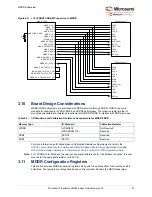
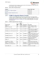
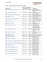
Page 72: ...e user must install the appropriate resistor on the PCB 3 11 MDDR Configuration Registers This section provides MDDR subsystem registers along with the address offset functionality and bit definitions...

Page 73: ...Register Summary Register Name Register Type Flash Write Protect Reset Source Description MDDR_CR RW P Register PORESET_N MDDR Configuration register MDDR_IO_CALIB_CR RW P Register PORESET_N MDDR I O...

Page 74: ...2_CR 0 028 RW PRESET_N DDRC Column Address Map register DDRC_ADDR_MAP_ROW_1_CR 0 02C RW PRESET_N DDRC Row Address Map register DDRC_ADDR_MAP_ROW_2_CR 0 030 RW PRESET_N DDRC Row Address Map register DD...

Page 75: ...er DDRC_MODE_REG_DATA_CR 0 080 RW PRESET_N DDRC Mode Register Write Data Register DDRC_PWR_SAVE_1_CR 0 084 RW PRESET_N DDRC Power Save register DDRC_PWR_SAVE_2_CR 0 088 RW PRESET_N DDRC Power Save reg...

Page 76: ...r SECDED Registers DDRC_SINGLE_ERR_CNT_STATUS_SR 0 0E8 RO PRESET_N DDRC single error count Status register DDRC_DOUBLE_ERR_CNT_STATUS_SR 0 0EC RO PRESET_N DDRC double error count status register DDRC_...

Page 77: ...SET_N DDRC last corrected error address register DDRC_LCB_NUMBER_SR 0 128 RO PRESET_N DDRC last corrected bit number register DDRC_LCB_MASK_1_SR 0 12C RO PRESET_N DDRC last corrected bit mask status r...

Page 78: ...when all other registers have been programmed Asserting this bit does NOT reset all the APB configuration registers Once the soft reset bit is asserted the APB register should be modified as required...

Page 79: ...s 0x0 Single refresh 0x1 Burst of 2 0x7 Burst of 8 refresh Table 32 DDRC_DYN_POWERDOWN_CR Bit Number Name Reset Value Description 31 2 Reserved 0 0 Software should not rely on the value of a reserved...

Page 80: ...0 0 Software should not rely on the value of a reserved bit To provide compatibility with future products the value of a reserved bit should be preserved across a read modify write operation 11 8 REG_...

Page 81: ...s field 7 4 REG_DDRC_ADDRMAP_COL_B4 0 0 Full bus width mode Selects column address bit 5 Half bus width mode Selects column address bit 6 Quarter bus width mode Selects column address bit 7 Valid Rang...

Page 82: ...et to 15 column address bit 9 is set to 0 7 4 REG_DDRC_ADDRMAP_COL_B1 0 0 0 Full bus width mode Selects column address bit 12 Half bus width mode Selects column address bit 13 Quarter bus width mode U...

Page 83: ...se to the value of this field 3 0 REG_DDRC_ADDRMAP_ROW_B12 0 0 Selects the address bit used as row address bit 12 Valid Range 0 to 11 and 15 Internal Base 18 The selected address bit is determined by...

Page 84: ...of a global timer that pulses every 32 clock cycles There is no known specific requirement for this It may be set to zero 7 1 REG_DDRC_FINAL_WAIT_X32 0 0 Cycles to wait after completing the DRAM init...

Page 85: ...read modify write operation 11 2 REG_DDRC_POST_CKE_X1024 0 0 Cycles to wait after driving CKE High to start the DRAM initialization sequence Units 1 024 clocks DDR Typically requires a 400 ns delay r...

Page 86: ...ller sets those bits appropriately Table 44 DDRC_INIT_EMR2_CR Bit Number Name Reset Value Description 31 16 Reserved 0 0 Software should not rely on the value of a reserved bit To provide compatibilit...

Page 87: ...al is present for designs supporting LPDDR1 DRAM only It is used to calculate when the DRAM clock may be stopped Table 48 DDRC_DRAM_RD_WR_PRE_CR Bit Number Name Reset Value Description 31 10 Reserved...

Page 88: ...f a reserved bit should be preserved across a read modify write operation 10 5 REG_DDRC_T_RAS_MAX 0 0 tRAS max Maximum time between activate and precharge to same bank Maximum time that a page can be...

Page 89: ...esh Unit clocks Table 53 DDRC_DRAM_BANK_ACT_TIMING_CR Bit Number Name Reset Value Description 31 14 Reserved 0 0 Software should not rely on the value of a reserved bit To provide compatibility with f...

Page 90: ...lay ODT setting should remain constant for the entire time that DQS is driven by the controller 3 2 REG_DDRC_RANK0_WR_ODT 0 0 0 Indicates which remote ODTs should be turned on during a write to rank 0...

Page 91: ...cycles when write requires changing ODT settings 11 Reserved Table 56 DDRC_ADDR_MAP_COL_3_CR Bit Numbe r Name Reset Value Description 31 16 7 6 Reserved 0 0 Software should not rely on the value of a...

Page 92: ...e critical word 0 Reserved 0 0 Software should not rely on the value of a reserved bit To provide compatibility with future products the value of a reserved bit should be preserved across a read modif...

Page 93: ...OWERDOWN_TO_X32 0 06 After this many clocks of NOP or DESELECT the controller puts the DRAM into power down This must be enabled in the Master Control register Unit Multiples of 32 clocks 0 REG_DDRC_C...

Page 94: ...value of a reserved bit should be preserved across a read modify write operation 9 0 REG_DDRC_T_ZQ_SHORT_NOP 0 0 Number of cycles of NOP required after a ZQCS ZQ calibration short command is issued to...

Page 95: ...ed bit should be preserved across a read modify write operation 7 0 REG_DDRC_T_ZQ_SHORT_INTERVAL_X1024 0 0 20 bits are split into two registers 19 12 bits of REG_DDRC_T_ZQ_SHORT_INTERVAL_X10 24 Averag...

Page 96: ...EG_DDRC_PAGECLOSE 0 0 1 Bank is closed and kept closed if no transactions are available for it This is different from auto precharge a Explicit precharge commands are used and not read write with auto...

Page 97: ...DDRC_HPR_QUEUE_PARAM_2_CR Bit Number Name Reset Value Description 31 11 Reserved 0 0 Software should not rely on the value of a reserved bit To provide compatibility with future products the value of...

Page 98: ...et Value Description 31 15 Reserved 0 0 Software should not rely on the value of a reserved bit To provide compatibility with future products the value of a reserved bit should be preserved across a r...

Page 99: ...ns to low priority implicitly turns off bypass Table 72 DDRC_PERF_PARAM_3_CR Bit Number Name Reset Value Description 31 1 Reserved 0 0 Software should not rely on the value of a reserved bit To provid...

Page 100: ...n 31 10 Reserved 0 0 Software should not rely on the value of a reserved bit To provide compatibility with future products the value of a reserved bit should be preserved across a read modify write op...

Page 101: ...31 6 Reserved 0 0 Software should not rely on the value of a reserved bit To provide compatibility with future products the value of a reserved bit should be preserved across a read modify write opera...

Page 102: ...Low when the MR write command is issued to the DRAM Any MR write command that is received when DDRC_REG_MR_WR_BUSY is High is not accepted Table 79 DDRC_SINGLE_ERR_CNT_STATUS_SR Bit Number Name Reset...

Page 103: ...following SECDED 71 64 SECDED 63 00 Data In the same clock cycle if one lane has a correctable error and the other lane has an uncorrectable error the syndrome for the uncorrectable error is sent on t...

Page 104: ...YNDROME_3_SR Bit Number Name Reset Value Description 31 16 Reserved 0 0 Software should not rely on the value of a reserved bit To provide compatibility with future products the value of a reserved bi...

Page 105: ...correctable error and the other lane has an uncorrectable error the syndrome for the uncorrectable error is sent on this bus If more than one data lane has an error in it the lower data lane is selec...

Page 106: ...C_LUE_ADDRESS_1_SR Bit Number Name Reset Value Description 31 15 Reserved 0 0 Software should not rely on the value of a reserved bit To provide compatibility with future products the value of a reser...

Page 107: ...correctable error and the other lane has an uncorrectable error the syndrome for the uncorrectable error is sent on this bus If more than one data lane has an error in it the lower data lane is select...

Page 108: ..._SYNDROME_3_SR Bit Number Name Reset Value Description 31 16 Reserved 0 0 Software should not rely on the value of a reserved bit To provide compatibility with future products the value of a reserved...

Page 109: ...correctable error and the other lane has an uncorrectable error the syndrome for the uncorrectable error is sent on this bus If more than one data lane has an error in it the lower data lane is selec...

Page 110: ...over by the system Table 93 DDRC_LCE_ADDRESS_1_SR Bit Number Name Reset Value Description 31 15 Reserved 0 0 Software should not rely on the value of a reserved bit To provide compatibility with futu...

Page 111: ...should not rely on the value of a reserved bit To provide compatibility with future products the value of a reserved bit should be preserved across a read modify write operation 15 0 DDRC_LCB_MASK 0 0...

Page 112: ...e compatibility with future products the value of a reserved bit should be preserved across a read modify write operation 15 0 DDRC_LCB_MASK 0 0 64 bits are split into four registers 47 32 bits of DDR...

Page 113: ...the value of a reserved bit To provide compatibility with future products the value of a reserved bit should be preserved across a read modify write operation 2 0 DDRC_ECC_STATUS_SR 0 0 Bit 0 1 Indic...

Page 114: ...FIFO RE generation One bit for each data slice 1 Data slice is valid 0 Read data responses are ignored Note The PHY data slice 0 must always be enabled Table 104 DDR_FIC Configuration Register Summar...

Page 115: ...n this register DDR_FIC_HPD_SW_WRB_EMPTY_S R 0 430 RO PRESET_ N Indicates valid data in read and write buffer for AHBL master1 and master2 DDR_FIC_SW_HPB_LOCKOUT_SR 0 434 RO PRESET_ N Write and read b...

Page 116: ...per DDR burst size This port is common for all buffers Buffers can be configured to 16 byte or 32 byte size 0 Buffer size is configured to 16 bytes 1 Buffer size is configured to 32 bytes 7 4 Reserved...

Page 117: ...for AHBL master1 0 Disable write buffer for AHBL master1 3 Reserved 0 0 Software should not rely on the value of a reserved bit To provide compatibility with future products the value of a reserved b...

Page 118: ...ation 8 DDR_FIC_LTO_CLR 0 0 Clear signal to lock timeout interrupt 7 5 Reserved 0 0 Software should not rely on the value of a reserved bit To provide compatibility with future products the value of a...

Page 119: ...2 bit AHB master implemented in fabric 1 Two 32 bit AHB masters implemented in fabric 3 0 Reserved 0 0 Software should not rely on the value of a reserved bit To provide compatibility with future prod...

Page 120: ...de compatibility with future products the value of a reserved bit should be preserved across a read modify write operation 15 0 DDR_FIC_M2_ERR_ADD 0 0 32 bits are split into two registers Lower 16 bit...

Page 121: ...r of AHBL master2 does not have valid data 0 Default 1 Reserved 0 0 Software should not rely on the value of a reserved bit To provide compatibility with future products the value of a reserved bit sh...

Page 122: ...h when error response is received for bufferable write request Goes Low when processor serves the interrupt Table 120 DDR_FIC_LOCK_TIMEOUTVAL_1_CR Bit Number Name Reset Value Description 31 16 Reserve...

Page 123: ...ntroller and Serial High Speed Controller Initialization Methodology 3 0 CFGR_LOCK_TIMEOUT_REG 0 0 20 bits are split into two registers 19 16 bits of CFGR_LOCK_TIMEOUT_REG Lock timeout 20 bit register...

Page 124: ...eatures Window The following steps describe how to configure the MDDR 1 Check the MSS External Memory check box under the Device Features tab select MDDR and leave the other check boxes unchecked The...

Page 125: ...be entered from 0 to 15 if the Arbitration Scheme selected other than Type 0 Address Mapping The register settings to perform mapping to system address bits for various Row Bank and Column combinatio...

Page 126: ...electing I O Standard as LVCMOS18 or LPDDRI 4 Depending on the application requirement select the Memory Initialization settings under the Memory Initialization tab as shown in Figure 50 on page 117 S...

Page 127: ...s of Full and Weak drive strength and it is defined by MR1 register bits M5 and M1 of DDR3 memory with drop down options of RZQ 6 and RZQ 7 Partial array self refresh coverage setting is defined by EM...

Page 128: ...igure 50 DDR Memory initialization Settings 5 Select the Memory Timing settings under the Memory Timing tab according to the DDR memory vendor datasheet as shown in the following illustration For more...

Page 129: ...configurations and the MDDR subsystem registers are initialized by the Cortex M3 processor during the system_init phase of the firmware projects SoftConsole IAR Keil projects generated by Libero SoC T...

Page 130: ...IC Subsystem and click configure to select the type of interface as AXI or single AHB Lite The user logic in the FPGA fabric can access the DDR memory through the MDDR using these interfaces The follo...

Page 131: ..._CLK can be configured as a ratio of MDDR_CLK 1 2 3 4 6 8 12 or 16 using the Clocks configurator The maximum frequency of DDR_FIC_CLK is 200 MHz The following image shows the DDR_FIC_CLK configuration...

Page 132: ...ing and DDR I O settings MDDR register initialization The MDDR subsystem registers can be initialized using the Cortex M3 processor or FPGA fabric master After MSS resets the MDDR registers must be co...

Page 133: ...ctions explain the configuration steps in the flow chart 3 12 2 1 MSS External Memory Configuration The MDDR subsystem is configured through the MDDR configurator which is part of the MSS configurator...

Page 134: ...tor will be displayed as shown in the following image Select the memory settings as described in the steps 2 3 and 4 in the Design Flow Using System Builder section on page 112 To access the MDDR from...

Page 135: ...Figure 60 MDDR Clock Configuration If the MDDR_CLK ratio to M3_CLK is a multiple of 3 DDR_SMC_FIC_CLK s ratio to MDDR_CLK must also be a multiple of 3 and vice versa The configurator issues an error...

Page 136: ...IC_2_APB_M_PCLK The FIC_2_APB_M_PCLK clock is generated from the MSS_CCC and is identical to M3_CLK 4 3 12 2 3 I O Configuration I O settings such as like ODT and drive strength can be configured as s...

Page 137: ...itialized The read write and read modify write transactions are initiated by the AXI master to read or write the data into the DDR memory after receiving the ready signal from APB master Figure 63 MDD...

Page 138: ...and chip oscillators in the SmartDesign canvas and configure as required 7 Instantiate user AXI master logic in the SmartDesign canvas to access the MDDR through the AXI interface Make sure that the A...

Page 139: ...actions Note The MDDR subsystem can be configured using the Cortex M3 processor without having an APB master The System Builder can be used to create the design by following steps in Design Flow Using...

Page 140: ...nterface To use a dual rather than single AHB interface to the MDDR set the CFG_NUM_AHB_MASTERS bit in the DDR_FIC_NUM_AHB_MASTERS_CR register to 1 DDR I O MSS DDR Bridge DDR SDRAM MSS MDDR AHB Lite S...

Page 141: ...master 12 One or two AHB masters must be connected through CoreAHB s in the SmartDesign canvas 3 12 5 Use Model 3 Accessing MDDR from Cortex M3 Processor The Cortex M3 processor can access the DDR SD...

Page 142: ...Figure 16 on page 40 shows the System Builder Device Features tab Figure 71 MSS External Memory Configuration 2 Navigate to Memories tab and import the DDR configuration file or select the appropriate...

Page 143: ...o initialize the MDDR registers 8 Simulate the design to verify the read write transactions to DDR memory 9 Open I O Attribute Editor to configure the ODT and drive strengths 10 Program the device 11...

Page 144: ...access DDR memory from the HPDMA through the MDDR The HPDMA driver has the MSS_HPDMA_start API to initiate memory transfers and DDR memory from and to other memory locations This API requires the para...

Page 145: ...sequential and interleaved burst ordering Programs internal control for ZQ short calibration cycles for DDR3 configurations Supports dynamic scheduling to optimize bandwidth and latency Supports self...

Page 146: ...wide range of common memory types configurations and densities as shown in the following table If SECDED mode is enabled in the FDDR controller the external memory module must be connected to the foll...

Page 147: ...cription of the FDDR subsystem with the following sub sections Architecture Overview Port List Initialization Details of Operation 4 5 1 Architecture Overview A functional block diagram of the FDDR su...

Page 148: ...XI transaction controller receives read and write requests from AXI masters DDR_FIC and schedules for the DDR controller by translating them into DDR controller commands The DDR controller receives th...

Page 149: ...l sideband signal and is valid with the AWVALID signal Only used when SECDED is enabled HPMS_DDR_FIC_SUBSYSTEM_CLK3 Out This output clock is derived from the FDDR_CLK and is based on the DDR_FIC divid...

Page 150: ...gh DRAM single ended data strobe output for bidirectional pads FDDR_DQS_ECC_N In out Low DRAM data input or output for bidirectional pads FDDR_DQS_TMATCH_0_IN In High DQS enables input for timing matc...

Page 151: ...igh Indicates that the slave is ready to accept an address and associated control signals 1 Slave ready 0 Slave not ready AXI_S_BID 3 0 Output Indicates response ID The identification tag of the write...

Page 152: ...transaction AXI_S_ARBURST 1 0 Input Indicates burst type The burst type coupled with the size information details how the address for each transfer within the burst is calculated 00 FIXED Fixed addres...

Page 153: ...normal sequential memory 10 WRAP Incrementing address burst that wraps to a lower address at the wrap boundary 11 Reserved AXI_S_AWID 3 0 Input Indicates identification tag for the write address group...

Page 154: ...ich byte lanes to update in memory AXI_S_WVALID Input High Indicates whether valid write data and strobes are available 1 Write data and strobes available 0 Write data and strobes not available Table...

Page 155: ...roller performs external DRAM memory reset and initialization as per the JEDEC specification including reset refresh and mode registers AHBx_S_HTRANS 1 0 Input Indicates AHB transfer type from Fabric...

Page 156: ...DT and Driver Impedance section of the I Os chapter in the UG0445 IGLOO2 FPGA and SmartFusion2 SoC FPGA Fabric User Guide Figure 76 Reset Sequence 4 6 2 ZQ Calibration ZQ calibration is applicable for...

Page 157: ...memory The TMATCH_OUT and TMATCH_IN signals are shorted close to the FPGA balls to remove the FPGA output and input delays from the round trip delay time Therefore the fixed delay ratios represent onl...

Page 158: ...ock assertion and deassertion 4 6 3 1 2 FACC Within the FDDR clock controller the FACC is responsible for interfacing with the FPLL generating the aligned clocks required by the FDDR subsystem and con...

Page 159: ...selected the DDR_FIC converts the single or dual 32 bit AHBL master transactions from the FPGA fabric to 64 bit AXI transactions The DDR bridge which is embedded as part of the DDR_FIC is enabled in t...

Page 160: ...port handles only one write transaction at a time and generates the handshaking signals on the AXI interface 4 6 3 3 2 Priority Block The priority block prioritizes AXI read write transactions and pro...

Page 161: ...bit that maps to each and every applicable DDR memory address bit The address map interface registers can be configured to map source address bits to DRAM address for more information refer to Address...

Page 162: ...erates an ECC_INT interrupt signal which can be monitored from FPGA fabric Sends the data with error to the read requested MSS HPMS and FPGA fabric master as part of the read data Sends the SECDED err...

Page 163: ...Os are tri stated only in self refresh mode Deep power down LPDDR1 This is supported only for LPDDR1 The DDR controller puts the DDR SDRAM devices in Deep Power down mode whenever the REG_DDRC_DEEPPOW...

Page 164: ...specification Dynamic DRAM constraints are subdivided into three basic categories Bank constraints affect the transactions that are scheduled to a given bank Rank constraints affect the transactions t...

Page 165: ...ommand to the same bank Read to precharge delay tRTP REG_DDRC_RD2PRE Table 48 page 76 Minimum time from a Read command to a precharge command to the same bank Set this to the current value of additive...

Page 166: ...ogrammed value for that register as described in the following equation Internal base register value source address bit number EQ 2 For example reading the description for REG_DDRC_ADDRMAP_COL_B3 the...

Page 167: ...em address bit 11 To map the column 3 bit C3 to address 5 the field is configured to 3 as the base value is 2 Similarly the other column address bits are configured DDRC_ADDR_MAP_COL_1_CR 0x3333 DDRC_...

Page 168: ...transactions to low priority configure the DDRC_PERF_PARAM_2_CR register Table 71 page 87 By default it is configured to force all the incoming transactions to low priority 4 6 10 5 Refresh Controls...

Page 169: ...can select the features that you require For details on how to launch the System Builder wizard and a detailed information on how to use it refer the IGLOO2 System Builder User s Guide You can also u...

Page 170: ...ent to CoreConfigIP through the FIC_2 master port CoreConfigP sends the configuration data to APB bus of the FDDR subsystem 3 Navigate to the Memories tab Depending on the application requirement sele...

Page 171: ...in the following image Select I O standard as LVCMOS18 or LPDDRI Note If LVCMOS18 is selected all IOs are configured to LVCMOS1 8 except CLK CLK_N CLK and CLK_N are configured to LPDDRI standard as t...

Page 172: ...is the delay in clock cycles between the internal READ command and the availability of the first bit of output data Select the CAS latency according to the DDR memory Mode register datasheet Select th...

Page 173: ...2 0 register bits of LPDDR memory with drop down options of Full Quarter One eighth and One sixteenth This feature helps in improving power savings during self refresh by selecting the amount of memor...

Page 174: ...igure 85 Memory Initialization Configuration 6 Select the memory timing settings under the Memory Timing tab according to the DDR memory vendor data sheet as shown in the following image For more deta...

Page 175: ...DR_Emcraft_Config zip An example of FDDR register configurations for operating the LPDDR memory MT46H64M16LF with clock 166 MHz is given below Device Memory Settling Time us 200 The DDR memories requi...

Page 176: ...ster core to the Fabric DDR Subsystem This allows to configure the type of interface as AXI single AHB Lite On completing the configuration the selected interface is enabled The user logic in the FPGA...

Page 177: ...h The following image shows the I O Editor window Figure 89 I O Editor Window 4 7 2 Accessing FDDR from FPGA Fabric through the AXI Interface The AXI master in the FPGA fabric can access the DDR memor...

Page 178: ...read from or write the data to the DDR memory after initializing the FDDR registers The following steps access the FDDR from the AXI master in the FPGA fabric FIC_0 FIC_1 AHB Bus Matrix D D R I O Fab...

Page 179: ...In this example the design is created to access the DDR3 memory with a 32 bit data width and no ECC 3 Set the DDR memory settling time to 200 us and then click Import Register Configuration Figure 92...

Page 180: ...g image shows the AMBA Master Configuration dialog Figure 94 AMBA Master Configuration 8 Configure the System Clock and Subsystem clocks in Clocks tab The following image shows the Clocks configuratio...

Page 181: ...terface Make sure that the AXI master logic accesses the FDDR after configuring the FDDR registers 12 Instantiate the CCC block in the SmartDesign canvas and configure it to generate 111 MHz clock 13...

Page 182: ...AXI throughput see AC422 SmartFusion2 Optimizing DDR Controller for Improved Efficiency Libero v11 7 Application Note 4 7 3 Accessing FDDR from FPGA Fabric through the AHB Interface The FDDR subsyste...

Page 183: ...FDDR Mode DDR3 Fabric Clock to FDDR Clock Ratio 1 4 PHY Width 16 and 32 Clock Frequency 80 MHz The other parameters are configured similar to the FDDR configuration in AC422 SmartFusion2 Optimizing D...

Page 184: ...R3 SDRAM connected to the FDDR of a IGLOO2 device Micron s MT41J512M8RA is a 512 MB density device with x8 data width The FDDR is configured in Full Bus Width mode with SECDED enabled The SDRAM connec...

Page 185: ...E CLK_P CLK_N CSN ODT RASN RSTN WEN ADDR 15 0 BA 2 0 MT41J512M8RA FDDR_CAS_N FDDR_CKE FDDR_CLK FDDR_CLK_N FDDR_CS_N FDDR_ODT FDDR_RAS_N FDDR_RESET_N FDDR_WE_N FDDR_ADDR 15 0 FDDR_BA 2 0 FDDR_DM_RDQS 0...

Page 186: ...ation on page 204 Table 142 Address Table for Register Interfaces Registers Address Offset Space DDR Controller Configuration Register Table 28 page 63 0x000 0x1FC PHY Configuration Register Summary T...

Page 187: ...K_DDR_FIC PLL_DELAY_LINE_SEL 0x518 RW P PRESETN Selects the delay values to be added to the FPLL FDDR_SOFT_RESET 0x51C RW P PRESETN Soft reset register for FDDR FDDR_IO_CALIB_CR 0x520 RW P PRESETN Con...

Page 188: ...LL is not in reset 2 0 PLL_OUTPUT_DIVISOR 0 2 Configures the amount of division to be performed on the internal multiplied PLL clock in order to generate the DDR clock Output divider value 000 1 001 2...

Page 189: ...perating range 10 7 PLL_LOCKCNT 0 F Configured to control the corresponding configuration input of the FPLL LOCK counter Value 2 binary value 5 0000 32 1111 1048576 For the number of reference cycles...

Page 190: ...exers are switched by one signal Allowed values 0 HPMS_CLK PCLK0 PCLK1 CLK_DDR_FIC all driven from stage 2 dividers from CLK_SRC 1 HPMS_CLK PCLK0 PCLK1 CLK_DDR_FIC all driven from CLK_STANDBY 6 FACC_P...

Page 191: ...vide compatibility with future products the value of a reserved bit should be preserved across a read modify write operation 7 5 BASE_DIVISOR 0 0 Selects the ratio between CLK_A and the regenerated ve...

Page 192: ...01 One buffer delay 10 Two buffers delay 11 Three buffers delay Table 151 FDDR_SOFT_RESET Bit Number Name Reset Value Description 31 2 Reserved 0 0 Software should not rely on the value of a reserved...

Page 193: ...reserved bit To provide compatibility with future products the value of a reserved bit should be preserved across a read modify write operation 6 DDR_FIC_INT_ENABLE 0 0 Masking bit to enable DDR_FIC i...

Page 194: ...ould not rely on the value of a reserved bit To provide compatibility with future products the value of a reserved bit should be preserved across a read modify write operation 0 FPLL_LOCK 0 0 Indicate...

Page 195: ..._CALIB_SR Bit Number Name Reset Value Description 31 Reserved 0 0 Software should not rely on the value of a reserved bit To provide compatibility with future products the value of a reserved bit shou...

Page 196: ...details on how to launch the System Builder wizard and detailed information on how to use it refer the SmartFusion2 System Builder User Guide For more information on DDR initialization refer to the S...

Page 197: ...can be enabled or disabled Address Mapping The register settings to perform mapping to system address bits for various Row Bank and Column combinations are automatically computed by the configurator...

Page 198: ...ote If LVCMOS18 is selected all IOs are configured to LVCMOS1 8 except CLK CLK_N CLK and CLK_N are configured to LPDDRI standard as they are differential signals Select I O calibration as ON or OFF If...

Page 199: ...Calibration section on page 145 Zqinit ZQCS ZQCS Interval Select other settings Local ODT setting is not supported for LPDDR memory For DDR2 DDR3 memory type user can choose any option for Local ODT...

Page 200: ...189 Figure 105 DDR Memory initialization Settings 5 Select the Memory Timing settings under the Memory Timing tab according to the DDR memory vendor datasheet as shown in the following image For more...

Page 201: ...SoC stores these configurations and the FDDR subsystem registers are initialized by the Cortex M3 processor during the system_init phase of the firmware projects SoftConsole IAR Keil projects generat...

Page 202: ...emory through the FDDR using these interfaces the following image shows the Peripherals tab Figure 107 MSS DDR FIC Subsystem Configuration 7 Navigate to the Clocks tab The Clocks tab allows to configu...

Page 203: ...and DDR I O settings FDDR register initialization FDDR subsystem registers can be initialized using the ARM Cortex M3 processor or FPGA fabric master After MSS reset the FDDR registers have to be conf...

Page 204: ...rtDesign to access the external DDR memory through the DDR Memory Controller subsystem The FDDRC macro configurator shown in the following image enables configuration of the DDR Memory Controller subs...

Page 205: ...ted interface is exposed in SmartDesign User logic in the FPGA fabric can access DDR memory through the FDDR using these interfaces The DDR_FIC clock drives the DDR_FIC slave interface and defines the...

Page 206: ...tween the APB configuration interface and FDDR subsystem Figure 111 FIC Configuration While enabling this option the APB_S_PCLK and FIC_2_APB_M_PCLK signals are exposed in SmartDesign The FDDR s APB_S...

Page 207: ...are initiated by the AXI master to read or write the data into the DDR memory after receiving a ready signal from the APB master Figure 113 FDDR with AXI Interface Use the following steps to access t...

Page 208: ...Revision 7 0 197 Figure 114 FDDR Configuration 3 Instantiate the clock resources FAB_CCC and chip oscillators in the SmartDesign canvas and configure as required In this example the fabric CCC is con...

Page 209: ...ing the FDDR registers from the APB master The AXI master clock frequency should be same as FDDR DDR_FIC clock frequency 5 Instantiate user APB master logic in the SmartDesign canvas to configure the...

Page 210: ...the fabric is used as AHB master 1 The FDDR registers are configured from the Cortex M3 processor through CoreConfigP The read write and read modify write transactions are initiated by the AXI master...

Page 211: ...0 clock is configured to 111 MHz Figure 119 MSS CCC Configuration 5 Instantiate the DDR Memory Controller macro in the SmartDesign canvas 6 Configure the FDDR and select the dual AHB interface as show...

Page 212: ...ication requirement select the memory settings For more details refer to 3 and 4 in the Design Flow Using System Builder 8 Instantiate the clock resources FCCC and chip oscillators in the SmartDesign...

Page 213: ...martDesign canvas and configure for FDDR as shown in the following image Make the FIC_2 and FDDR APB interface connections to CoreConfigP Figure 122 CoreConfigP IP Configuration 10 Instantiate CoreRes...

Page 214: ...o access the FDDR through the AHB interface The AHB master clock frequency should be the same as the FDDR DDR_FIC clock frequency 12 Connect the AHB master to the FDDR AHB slave0 interface through Cor...

Page 215: ...ck bits are set in a text txt file which is then imported into the SmartFusion2 project 4 11 1 Lock Bit File An initial default lock bit file can be generated by clicking Generate FPGA Array Data in t...

Page 216: ...ration file Figure 125 Lock Bit Configuration File 4 11 3 Locking and Unlocking a Register A register can be locked or unlocked by setting the appropriate lock bit value in the lock bit configuration...

Page 217: ...Fabric DDR Subsystem Microsemi ProprietaryUG0446 User Guide Revision 7 0 206 4 Regenerate the bitstream...

Page 218: ...ridge in the FDDR shown in blue subsystem facilitates fabric masters to access DDR memory Figure 127 DDR Bridges in the SmartFusion2 IGLOO2 FPGA Device The DDR bridge supports a single 64 bit AXI and...

Page 219: ...fore bursting out to external DDR memory It also includes read buffers for AHB masters to efficiently read data from the external DDR memory All buffers within the DDR bridge are implemented with latc...

Page 220: ...d if buffering is not required The WCB has a 10 bit timer down counter which starts when the first bufferable write data is loaded into the WCB The timer starts decrementing its value at every positiv...

Page 221: ...regardless of the size of request from the master Each read buffer is associated with one specific master for reading it does not check the read addresses of other masters to determine whether that da...

Page 222: ...from a single master have a dedicated master ID Combinations of fixed and round robin priorities are assigned to the following masters Master Interface 1 Fixed first priority Master Interface 0 is re...

Page 223: ...ition The counter starts counting when a locked transaction is initiated on the bus When the counter reaches its maximum value an interrupt is generated The interrupt can be cleared by setting the DDR...

Page 224: ...ing to other values enter a 10 bit hexadecimal value in the provided field of DDR bridge configurator Select timeout value to a non zero value for buffering the write transactions Non bufferable regio...

Page 225: ...rable size using the DDR_FIC_NBRWB_SIZE_CR register Configure the timeout value for each write buffer using the DDR_FIC_LOCK_TIMEOUTVAL_1_CR and DDR_FIC_LOCK_TIMEOUTVAL_2_CR registers Set the timeout...

Page 226: ...for a detailed description of each register and bit Table 164 SYSREG Control Registers Register Name Register Type Flash Write Protect Reset Source Description DDRB_BUF_TIMER_CR RW P Register SYSRESE...

Page 227: ...enu has the options to select the region from 64 KB to 1 GB It also has an option none to select the complete memory as bufferable The default selection is 64 KB Non bufferable region address The base...

Page 228: ..._RW_EN_CR register Configure buffer size to 32 bytes or 16 bytes using the DDR_FIC_NBRWB_SIZE_CR register Configure the non bufferable address using the DDR_FIC_NB_ADD register Configure the non buffe...

Page 229: ...on bufferable region selection provides high throughput than bufferable For example when Cortex M3 processor fetches the data from data region that is stack and the application has bulk data transacti...

Page 230: ...the MSS HPMS If the SMC_FIC is enabled the MDDR subsystem will not be available In SMC_FIC mode the DDRIOs associated with the MDDR subsystem are available for user applications The following illustra...

Page 231: ...HB mode for the devices M2GL005 M2GL010 and M2GL025 For other devices it configures the SMC_FIC in AXI mode 6 1 1 Port List The following two tables show the 64 bit AXI and 32 bit AHBL port lists Note...

Page 232: ...mation 1 Master ready 0 Master not ready MDDR_SMC_AXI_M_AWREADY Input High Indicates that the slave is ready to accept an address and associated control signals 1 Slave ready 0 Slave not ready MDDR_SM...

Page 233: ...ss burst FIFO type 01 INCR Incrementing address burst normal sequential memory 10 WRAP Incrementing address burst that wraps to a lower address at the wrap boundary 11 Reserved MDDR_SMC_AXI_M_AWID 3 0...

Page 234: ...h transfer within the burst is calculated 00 FIXED Fixed address burst FIFO type 01 INCR Incrementing address burst normal sequential memory 10 WRAP Incrementing address burst that wraps to a lower ad...

Page 235: ...access okay 10 Slave error 11 Decode error MDDR_SMC_AXI_M_BRESP 1 0 Input Indicates write response This signal indicates the status of the write transaction 00 Normal access okay 01 Exclusive access o...

Page 236: ...s on how to launch the System Builder wizard and a detailed information on how to use it refer the IGLOO2 System Builder User Guide Figure 140 HPMS External Memory Configurator For more information on...

Page 237: ...r Guide Revision 7 0 226 Figure 141 HPMS SMC_FIC Subsystem Configuration 3 Configure CoreSDR_AXI to match the external memory parameters Figure 142 CoreSDR_AXI Configuration 4 Navigate to the Memory M...

Page 238: ...application and contains the following sub sections Design Flow Use Model 1 Accessing SDRAM from MSS Through CoreSDR_AXI 6 4 1 Design Flow The SMC_FIC can be enabled and configured through the MSS ext...

Page 239: ...omponents to meet application needs using MSS configurator 3 Configure the external memory interface type and select Using an AXI Interface as shown in the previous image 4 Instantiate and configure C...

Page 240: ...229 Figure 145 Subsystem Connections in SmartDesign Refer to the Accessing External SDRAM through Fabric tutorial which describes the steps for creating a design that accesses external SDR memory fro...

Reviews: