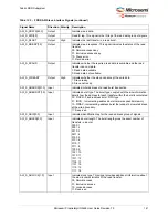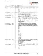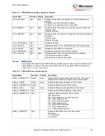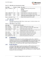
Fabric DDR Subsystem
Microsemi ProprietaryUG0446 User Guide Revision 7.0
149
4.6.3.3
AXI Transaction Controller
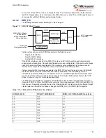
The AXI transaction controller receives 64-bit AXI transactions from DDR_FIC and translates them into
DDR controller transactions. The following illustration shows the block diagram of the AXI transaction
controller interfaced with the DDR controller.
Figure 78 •
AXI Transaction Controller Block Diagram
The AXI transaction controller comprises four major blocks:
•
AXI slave interface
•
Priority block
•
Transaction handler
•
Reorder buffer
4.6.3.3.1
AXI Slave Interfaces
The AXI transaction controller has a 64-bit AXI slave interface from DDR_FIC. The AXI slave port is
64 bits wide and is in compliance with the standard AXI protocol. Each transaction has an ID related to
the master interface. Transactions with the same ID are completed in order, while the transactions with
different read IDs can be completed in any order, depending on when the instruction is executed by the
DDR controller. If a master requires ordering between the transactions, the same ID should be used.
The AXI slave interface has individual read and write ports. The read port queues read AXI transactions
and it can hold up to four read transactions. The write port handles only one write transaction at a time
and generates the handshaking signals on the AXI interface.
4.6.3.3.2
Priority Block
The priority block prioritizes AXI read/write transactions and provides control to the transaction handler.
AXI read transactions have higher priority. The fabric master through DDR_FIC can be programmed to
have a higher priority by configuring the PRIORITY_ID and PRIORITY_ENABLE_BIT bit fields in the
DDRC_AXI_FABRIC_PRI_ID_CR register,
4.6.3.3.3
Transaction Handler
The transaction handler converts AXI transactions into DDR controller commands. The transaction
handler works on one transaction at a time from the read/write port queue that is selected by the priority
block. The transaction handler has a write command controller and read command controller for write
and read transactions.
The write command controller fetches the command from the AXI slave write port and sends a pure write
instruction to the DDR controller. If SECDED is enabled, a read modified write (RMW) instruction is sent
to the DDR controller. The read command controller generates read transactions to the DDR controller.
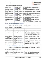
11
001
6:1
11
010
12:1
Table 132 •
FDDR_CLK to FPGA Fabric Clock Ratios
(continued)
DIVISOR_A[1:0]
DDR_FIC DIVISOR[2:0]
FDDR_CLK: FPGA FABRIC Clock Ratio
AXI Slave
Interface
Priority Block
Transaction
Handler
Re-Order Buffer
DDR
Controller
AXI Transaction Controller
PHY
64-Bit AXI Bus
from DDR_FIC

