MEN Mikro Elektronik A14C - 6U VME64 MPC8540 User Manual Download Page 117

Organization of the Board

MEN Mikro Elektronik GmbH

117

20A014-00 E2 – 2007-08-16

5.4

PCI Devices on Bus 0
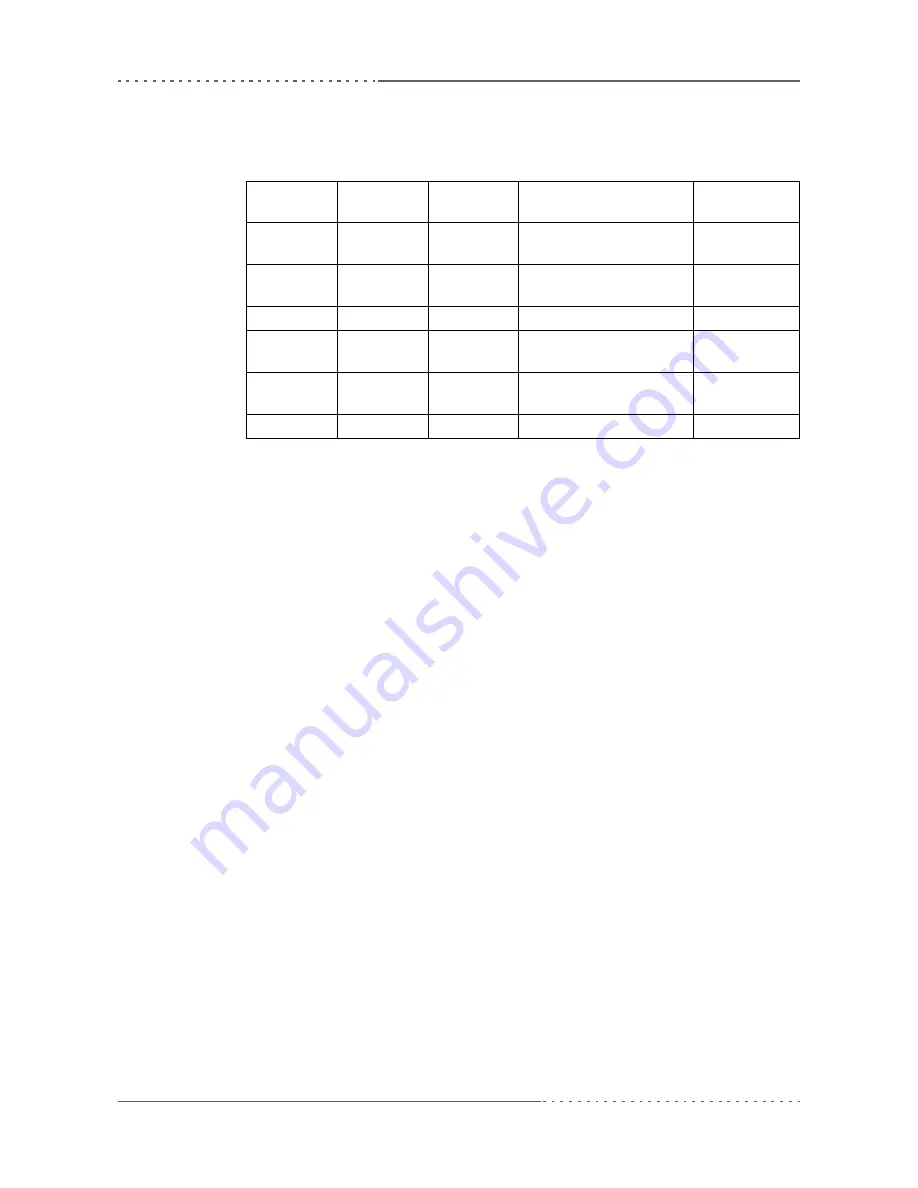
Table 60. 

PCI devices on Bus 0

Device 

Number

Vendor ID

Device ID

Function

Interrupt

0x00

0x1057

0x0008

PCI host bridge in 
MPC8540

-

0x14

0x3388

0x0026

PCI-to-PCI bridge

INTA, INTB, 
INTC, INTD

0x15

0x1172

0x5056

PCI-to-VMEbus bridge

INTB

0x16

0x1415

0x9501

Quad UART COM20..23 
(function no. 0)

INTC

0x16

0x1415

0x9511

Quad UART COM20..23 
(function no. 1)

INTD

0x1D

0x1172

0x4D45

FPGA

-

Summary of Contents for A14C - 6U VME64 MPC8540

Page 1: ...Embedded Solutions A14C 6U VME64 MPC8540 SBC PMC 20A014 00 E2 2007 08 16 User Manual Configuration example...

Page 2: ...ne fast Ethernet and one COM via four RJ45 connectors Four more UARTs are optionally accessible via SA Adapters for front connection Additional functionality such as graphics touch CAN binary I O etc...

Page 3: ...video data and NAND Flash firmware 8MB boot Flash 32KB non volatile FRAM Serial EEPROM 4kbits for factory settings Mass Storage Parallel IDE PATA One port for hard disk drives Drive can be connected...

Page 4: ...controlled Accessible via rear I O Front Connections Three Ethernet RJ45 COM1 RJ45 COM20 COM23 optional instead of PMC modules or in second front panel slot PMC 0 and 1 Rear I O COM10 GPIO Mezzanine...

Page 5: ...fast SRAM DMA Mailbox functionality Interrupter D08 O I 7 1 ROAK Interrupt handler D08 O IH 7 1 Single level 3 fair requester Single level 3 arbiter Bus timer Location Monitor Performance Coupled read...

Page 6: ...ing Altitude 300m to 3 000m Shock 15g 11ms Bump 10g 16ms Vibration sinusoidal 2g 10 150Hz Conformal coating on request Safety PCB manufactured with a flammability rating of 94V 0 by UL recognized manu...

Page 7: ...n SO DIMM EEPROM RTC Watchdog Ethernet 1000Base T Ethernet 1000Base T Ethernet 100Base T RS232 COM1 F F F FPGA VME P2 VME P1 SDRAM Additional NAND Flash Quad UART COM20 23 B PCI toPCI Bridge PCI to VM...

Page 8: ...to maximum available Additional SDRAM 0 MB or 16 MB FRAM 0 MB or 32 MB Boot Flash 8 MB or 16 MB I O Quad UART COM20 23 Direct on board connection via 10 pin connectors instead of PMCs Front Connectio...

Page 9: ...res MEN has a large number of standard IP cores to choose from Examples IDE e g PIO mode 0 UDMA mode 5 UARTs CAN bus Display control For IP cores developed by MEN please refer to our IP core overview...

Page 10: ...ons whenever you work on your computer Power down and unplug your computer system when working on the inside Hold components by the edges and try not to touch the IC chips leads or cir cuitry Use a gr...

Page 11: ...bers listings C function descriptions or wherever appropriate Hexadecimal numbers are preceded by 0x Hyperlinks are printed in blue color The globe will show you where hyperlinks lead directly to the...

Page 12: ...nc and SBS Technologies Inc MEN Mikro Elektronik ESMexpress and the MEN logo are registered trademarks of MEN Mikro Elektronik GmbH Altera Avalon Cyclone Nios and Quartus are trademarks or registered...

Page 13: ...Local PCI Bus 26 2 5 3 PCI to PCI Bridge 26 2 5 4 PCI to VMEbus Bridge 26 2 6 Memory 27 2 6 1 DRAM System Memory 27 2 6 2 Boot Flash 27 2 6 3 NAND Flash 27 2 6 4 FRAM 27 2 6 5 Additional SDRAM 27 2 6...

Page 14: ...onitor 72 2 16 15 DMA Controller 74 2 16 16 Connection 76 3 FPGA 82 3 1 General 82 3 2 System Unit 83 3 2 1 Functional Description 83 3 2 2 Address Organization 85 3 3 Standard Factory FPGA Configurat...

Page 15: ...6 4 MENMON Memory Map 105 4 6 5 MENMON BIOS Logical Units 106 4 6 6 System Parameters 107 4 7 MENMON Commands 113 5 Organization of the Board 115 5 1 Memory Mappings 115 5 2 Interrupt Handling 116 5 3...

Page 16: ...Installing SA Adapters on A14C directly 43 Figure 5 Position of fuse for COM20 COM23 protection 44 Figure 6 Installing a PMC mezzanine module 47 Figure 7 Position of reset button 51 Figure 8 FPGA Bloc...

Page 17: ...nment of I O connector J2 factory standard FPGA configuration 49 Table 15 Signal mnemonics of I O connector J2 factory standard FPGA configuration 50 Table 16 VMEbus interface PCI configuration space...

Page 18: ...MENMON Controller Logical Units CLUNs 106 Table 47 MENMON Device Logical Units DLUNs 106 Table 48 MENMON A14C system parameters autodetected parameters 107 Table 49 MENMON A14C system parameters prod...

Page 19: ...board and some hints for first installation 1 1 Maps of the Board Figure 1 Map of the Board front view A14c Standard Alternative COM20 23 via 10 pin connectors PMC 1 PMC 0 LAN2 A L LAN3 A L LAN1 A L C...

Page 20: ...lso incorporates the SO DIMM SDRAM Figure 2 Map of the Board top view Hard disk on adapter card J1 PCI 104 J2 I O SO DIMM MPC8540 LAN1 LAN2 LAN3 COM1 Heat Sink Plug on Module facing in VMEbus P2 VMEbu...

Page 21: ...up to four additional COM interfaces COM20 23 MEN provides a range of standard adapters and a mounting kit for four 9 pin D Sub connectors accessible through a second front panel Please see MEN s webs...

Page 22: ...___________________ Secondary MENMON for MEN EM3 Family 1 3 _________________ c 2005 2005 MEN Mikro Elektronik GmbH Nuremberg MENMON 2nd Edition Created Nov 18 2005 15 57 50 __________________________...

Page 23: ...ge 93 Observe the installation instructions for the respective software 1 4 Installing Operating System Software The board supports VxWorks Linux and QNX By standard no operating system is installed o...

Page 24: ...hes automatically from 56 s after reset to 1 6 s after the first trigger pulse This allows a longer watchdog timeout period during the start up phase After power up the CPU loads the FPGA The configur...

Page 25: ...e and software debugging support The second block is the Communications Processor Module CPM The CPM of the PowerQUICC III can support three fast serial communications controllers FCCs two multichanne...

Page 26: ...64 bit 66 MHz PCI bus operation is available on request In this case rows C and D of board to board connector J2 are used for the 64 bit extension signals See Chapter 2 14 Board to Board I O Connector...

Page 27: ...ins the boot software for the MENMON operating system bootstrapper and application software The MENMON sectors are software protected against illegal write transactions through a password in the seria...

Page 28: ...two devices For ordering options please see MEN s website The 44 pin IDE connector is located at the top side of A14C The pinning of the IDE connector complies with the ATA 4 ATAPI specification Conn...

Page 29: ...fast Size 1206 MEN part number 5675 0003 The fuse is located on the top side of A14C Figure 3 Position of fuse for IDE protection Signal Direction Function 5V out 5V power supply current limited to 3...

Page 30: ...s the space usually used for PMC slot 0 or for SA Adapters on COM20 and COM21 See Figure 2 Map of the Board top view on page 20 The board needs only one slot in the system even with a hard disk instal...

Page 31: ...007 08 16 Plug the hard disk adapter card to the 44 pin IDE connector on A14C Fasten the hard disk adapter card to A14C at the bottom side of the A14C using the four recess screws M2 5x4 and suitable...

Page 32: ...ch connector are accommodated at the front The pin assignments correspond to the Ethernet specification IEEE802 3 Table 3 Signal mnemonics of Ethernet 10Base T 100Base TX 1000Base TX interfaces Connec...

Page 33: ...ypes 9 pin D Sub plug according to DIN41652 MIL C 24308 with thread bolt UNC 4 40 Mating connector 9 pin D Sub receptacle according to DIN41652 MIL C 24308 available for rib bon cable insulation pierc...

Page 34: ...coaxial cable used for the 10Base 2 or 10Base 5 standards Since it is also cheaper it is the preferable solution for cost sensitive applications Cables in the 10Base T system connect with RJ45 connect...

Page 35: ...40 DUART 0 Table 7 Signal mnemonics of UART COM1 interface Connection via RJ45 Connector Connector types Modular 8 8 pin mounting jack according to FCC68 Mating connector Modular 8 8 pin plug accordin...

Page 36: ...re routed to one D Sub connector Connector types 9 pin D Sub plug according to DIN41652 MIL C 24308 with thread bolt UNC 4 40 Mating connector 9 pin D Sub receptacle according to DIN41652 MIL C 24308...

Page 37: ...u can use SA Adapters on a suitable transition module Please contact MEN s sales team if you have special needs For the pin assignment please see Table 30 Pin assignment of VMEbus rear I O connector P...

Page 38: ...Adapter connectors at the front are an option and are only available on request If all of those SA Adapter ports are implemented on A14C you cannot use any PMC slots Also COM20 and COM21 would collid...

Page 39: ...onnector types 40 pin low profile plug 2 54mm pitch for ribbon cable connection Mating connector 40 pin IDC receptacle e g Elco Series 8290 IDC socket Table 11 Pin assignment of the 40 pin UART COM20...

Page 40: ...SA Adapters in a different way than described in MEN s documentation Perform the following steps to install standard SA Adapters using MEN s SA Adapter mounting kit Power down your system and remove t...

Page 41: ...connector Make sure to always align the pins correctly pin 1 is marked by a triangle on the ribbon cable connector Use the SA Adapter s front panel screws to fasten the adapter at the additional fron...

Page 42: ...nnector at the front Note Please note that you can install adapters on the A14C directly only if you have a suitable version of A14C without PMC slots Perform the following steps to install an SA Adap...

Page 43: ...put it down making sure that the connectors are properly aligned Press the SA Adapter firmly onto the A14C Screw the SA Adapter tightly to the A14C using the front panel and standoff screws removed b...

Page 44: ...intended to be exchanged by the customer Your warranty for the A14C will cease if you exchange the fuses on your own Please send your board to MEN for repair if a fuse blows Current rating 1 5A Type f...

Page 45: ...ontrollers The GPIO signals are available via rear I O on connector P2 For the pin assignment please see Table 30 Pin assignment of VMEbus rear I O connector P2 FPGA I O signals on page 80 Since all o...

Page 46: ...layout is fully compatible to the IEEE1386 specification For connector pinouts please refer to the specification see Chapter 6 1 Literature and Web Resources on page 118 PMC slot 0 supports rear I O...

Page 47: ...f the PCBs facing each other Put the PMC module s front connector through the A14C s front slot at a 45 angle Carefully put it down making sure that the connectors are properly aligned Press the PMC m...

Page 48: ...that is used on model 01A014C00 See also Chapter 3 3 Standard Factory FPGA Configuration on page 92 This version of the A14C provides the following interfaces IDE UART COM10 GPIO 40 lines Miscellaneou...

Page 49: ...E_D12 GND GPIO_0 5 11 5V IDE_D13 GPIO_0 4 GND 12 IDE_D1 5V GPIO_0 6 GPIO_0 7 13 IDE_D0 IDE_D14 5V GPIO_1 1 14 GND IDE_D15 GPIO_1 0 5V 15 GND GPIO_1 2 GPIO_1 3 16 IDE_WR GPIO_3 2 GND GPIO_1 5 17 3 3V G...

Page 50: ...out IDE chip select 1 IDE_CS3 out IDE chip select 3 IDE_D 15 0 in out IDE data 15 0 IDE_IRQ in IDE interrupt request IDE_RD out IDE read strobe IDE_RDY in IDE ready IDE_RST out IDE reset IDE_WR out ID...

Page 51: ...unctional Description MEN Mikro Elektronik GmbH 51 20A014 00 E2 2007 08 16 2 15 Reset Button A reset button is integrated in the A14C s front panel handle Figure 7 Position of reset button Reset butto...

Page 52: ...ss and data transfer modes Master D08 EO D16 D32 D64 A16 A24 A32 ADO BLT RMW Slave D08 EO D16 D32 D64 A16 A24 A32 BLT RMW Interrupt handler 7 level D08 O IH 7 1 Interrupter 7 level D08 O I 7 1 ROAK Si...

Page 53: ...1172 0x04 Status Register Command Register 0x08 Class Code 0x068000 Revision ID currently 0x01 0x0C BIST Header Type Latency Timer Cache Line Size 0x10 Base Address Register 0 0x14 Base Address Regist...

Page 54: ...ontroller Register r w 0x 001C LONGADD Upper 3 Address Bits for A32 r w 0x 0020 MAIL_IRQE Mailbox Interrupt Enable Register r w 0x 0024 MAIL_IRQ Mailbox Interrupt Request Register r w 0x 0028 PCI_OFFS...

Page 55: ...ce 0x 0101 0000 0x 0101 FFFC 64KB VME A16 D32 short space 0x 0140 0000 0x 014F FFFC 1MB Local SRAM 0x 0180 0000 0x 0180 0044 72 bytes VME Bridge Control Registers 0x 01C0 0000 16 bytes VME IACK space...

Page 56: ...The size of the A24 A32 windows is configurable in the corresponding Mask Registers Table 23 VMEbus slave address windows 2 16 5 SRAM The SRAM is accessible from the PCI and VMEbus side From the VMEbu...

Page 57: ...ow are enabled Generation of SYSRES Generation of SYSCLK not provided during slot 1 detection cycle Level 3 arbitration Bus arbitration timeout 250 s Bus transfer timeout 125 s The timeouts cannot be...

Page 58: ...bus not supported 0 1 Delayed write access to VMEbus default Posted write access to VMEbus IBERREN Interrupt Bus Error Enable 0 1 Local interrupt disabled if VMEbus bus error occurs default Local inte...

Page 59: ...st transfer the byte enables may change from one data portion to the next This must be taken into account when exchanging data with the SRAM Table 24 VMEbus interface valid combinations for byte enabl...

Page 60: ...15 D8 D31 D24 D7 D0 1 0 0 0 1 0 0 0 D7 D0 D31 D24 D15 D8 D23 D16 D23 D16 D15 D8 0 1 0 0 0 0 0 0 D7 D0 D31 D24 D15 D8 D23 D16 D23 D16 D15 D8 D31 D24 D7 D0 0 0 0 0 D64 0 0 0 0 D7 D0 D63 D56 D15 D8 D55 D...

Page 61: ...Atomic Operations CPU to SRAM Operations Not supported CPU to VME Operations Read Modify Write operations to the VMEbus can be done via bit RMW in the MSTR Master Control Register 0x0010 read write On...

Page 62: ...gister A24 0x0014 read write SLV16 Slave Control Register A16 0x0030 read write 15 12 11 8 SLMASK24 19 16 SLBASE24 19 16 7 5 4 3 0 SLEN24 SLBASE24 23 20 SLMASK24 Slave Base Address Mask Bits The size...

Page 63: ...f the A32 Slave window can be set to 00000000 10000000 11000000 11100000 11110000 11111000 11111100 11111110 11111111 256 MB 128 MB 64 MB 32 MB 16 MB 8 MB 4 MB 2 MB 1 MB Default 00000000 SLEN32 0 1 Sl...

Page 64: ...SK24_PCI Slave Base Address Mask Bits The size of the A24 PCI Slave window can be set to 0000 1000 1100 1110 1111 1 MB 512 KB 256 KB 128 KB 64 KB Default 0000 SLEN24_PCI 0 1 Slave Unit disabled defaul...

Page 65: ...11000 11111100 11111110 11111111 256 MB 128 MB 64 MB 32 MB 16 MB 8 MB 4 MB 2 MB 1 MB Default 00000000 SLEN32_PCI 0 1 Slave Unit disabled default Slave Unit enabled SLBASE32_PCI Slave s Base Address fo...

Page 66: ...4 Standard non privileged data access 0x3C H H H H L L A24 supervisory 64 bit block transfer MBLT 0x38 H H H L L L A24 non privileged 64 bit block transfer MBLT 0x29 H L H L L H A16 non privileged acc...

Page 67: ...the Release On Request ROR or Release When Done RWD scheme ROR should be preferred in single VMEbus master systems to increase the transfer rate Both register schemes are implemented as fair requeste...

Page 68: ...Status Register 0x0008 read write IMASK Interrupt Mask Register 0x000C read write ISTAT Interrupt Status Register 0x0008 read write In order to read the interrupt STATUS ID from the interrupter the CP...

Page 69: ...only when the INTEN bit is set INTEN should be set after the ILx bits are set to avoid glitches on the IRQ lines INTEN is automatically cleared during the acknowledge cycle and the request is removed...

Page 70: ...r way in order to address the entire VMEbus address space Therefore a register contains the upper three address bits LONGADD Upper 3 Address Bits for A32 0x001C read write 7 3 2 1 0 ADDR31 ADDR30 ADDR...

Page 71: ...IEVR2 IEVW1 IEVR1 IEVW0 IEVR0 IEVWx VMEbus write access to mailbox register x generates an interrupter request on the PCI bus when this bit is set Default 0x0 interrupt disabled This bit can be set an...

Page 72: ...4 and 3 of VMEbus address stored when location monitor found hit LOC_WR_x 0 1 Write accesses are not monitored Write accesses are monitored LOC_RD_x 0 1 Read accesses are not monitored Read accesses...

Page 73: ...write 31 0 ADDR 31 0 ADDR 31 0 Compare address for location monitor The desired address bits depend on LOC_AM_0 LOC_AM_0 0 0 LOCADDR_0 31 10 LOC_AM_0 1 0 LOCADDR_0 15 10 LOC_AM_0 1 1 LOCADDR_0 23 10...

Page 74: ...s is 16 The DMA controller is able to transfer data from the SDRAM to the VMEbus and vice versa For this reason source and or destination address can be incremented or not depending on the settings Th...

Page 75: ...pace Source is located in PCI address space not supported DMA_DEST_DEVICE 0 0 1 0 1 0 1 0 0 Destination is located in SRAM address space Destination is located in VME address space Destination is loca...

Page 76: ...nector P1 Z A B C D 1 D0 BBSY D8 2 GND D1 BCLR D9 GND 3 D2 ACFAIL D10 4 GND D3 BG0IN D11 5 D4 BG0OUT D12 6 GND D5 BG1IN D13 7 D6 BG1OUT D14 8 GND D7 BG2IN D15 9 GND BG2OUT GND GAP 10 GND SYSCLK BG3IN...

Page 77: ...nnector P2 while FPGA signals need to be switched through to the P2 connector When signals from the FPGA are led to P2 some of them overlap with PMC I O signals If you use FPGA I O signals e g COM10 G...

Page 78: ...12 GND PMC0_J4 24 GND PMC0_J4 23 13 PMC0_J4 26 5V PMC0_J4 25 14 GND PMC0_J4 28 D16 PMC0_J4 27 15 PMC0_J4 30 D17 PMC0_J4 29 16 GND PMC0_J4 32 D18 PMC0_J4 31 17 PMC0_J4 34 D19 PMC0_J4 33 18 GND PMC0_J4...

Page 79: ...16 Table 29 Signal mnemonics of VMEbus rear I O connector P2 PMC 0 Signal Direction Function Power 5V 5V power supply GND Digital ground VME64 A 31 24 in VME64 address lines D 31 16 in out VME64 data...

Page 80: ...J4 16 A28 GPIO_0 0 9 PMC0_J4 18 A29 GPIO_0 2 GPIO_0 3 10 GND PMC0_J4 20 A30 GPIO_3 5 GPIO_0 5 11 PMC0_J4 22 A31 GPIO_0 4 12 GND PMC0_J4 24 GND GPIO_0 6 GPIO_0 7 13 PMC0_J4 26 5V PMC0_J4 25 GPIO_1 1 14...

Page 81: ...A14C system Power on the A14C again The relevant commands to control the signals on the A14C s P2 connector are as follows Signal Direction Function COM10 CTS10 in Clear to send DCD10 in Data carrier...

Page 82: ...ecessity in the actual implementation and cannot be described in general Figure 8 FPGA Block diagram The FPGA System Unit contains a configuration table providing the information which modules are imp...

Page 83: ...dule which generates the interrupt by writing 1 or 0 to the corresponding bit of the module s interrupt enable register The CPU has to reset an interrupt request in the module which generates the inte...

Page 84: ...and output a 16 bit counter controls an output enable signal The counter value 0x1 switches the port to an input all other values force the port to act as an output The reset controller contains a sy...

Page 85: ...e CT r 0x0080 Interrupt Request Register IRQR r 0x0088 Reset Cause Register RCR r 0x008C Watchdog Timer Register WDTR r w 0x0090 Watchdog Value Register WDVR r w 0x0094 System Unit Control Register SU...

Page 86: ...larger than 256 bytes If other BARs are used the module s memory space which is allocated with the BARs other than BAR 0 has other base addresses as viewed from the PCI bus Inside the board s FPGA the...

Page 87: ...To reset a bit of the RCR the CPU has to write 1 acknowledge to the corresponding bit Reset value Module will not be reset by any reset only by configuration of FPGA Config Value 0x0000 15 14 13 12 11...

Page 88: ...ck Example The watchdog expiration time can be calculated by the following equation Example Watchdog expiration time 000000000111111bin This calculation leads to a user configurable watchdog expiratio...

Page 89: ...interrupt request from the reset controller by setting bit RCIREN to 1 or 0 and offers the possibility to reset the A14C through a CPU register access bit SW_RST Writing 1 to bit SW_RST forces a reset...

Page 90: ...rved HB SW_RST RCIREN PS_DEG_EN 0 Power supply overtemperature warning interrupt disabled 1 Power supply overtemperature warning interrupt enabled PS_FAL_EN 0 Power supply powerfail interrupt disabled...

Page 91: ...ead write The GPMR is an 8 bit register that the programmer can use to store data which will not be changed during a reset phase The register can be read from and written to by the programmer Only pow...

Page 92: ...I O connector 3 3 2 FPGA Configuration Table The resulting configuration table of the standard FPGA is as follows Note 16Z070_IDEDISK consists of three cores 16Z053_IDEATA 16Z068_IDETGT not implement...

Page 93: ...pplicable PCI auto configuration Perform self test Provide debug diagnostic features on MENMON command line Interaction with the user via touch panel TFT display if supported by FPGA 1 Boot operating...

Page 94: ...alid EarlyInit Secondary MENMON Secondary MENMON valid Check for D pressed Parse SO DIMM SPD Init DRAM Check for d pressed Quick DRAM test DegradedStartup Relocating DRAM ok Determine clocks I2C contr...

Page 95: ...line MenmonCli No user intervention User abort or degraded mode User abort or Self test error and stignfault false Execute mmstartup string mmstartup empty Jump to bootstrapper Booting do start networ...

Page 96: ...asured from the beginning of the self test even if the actual test has finished earlier to give the user a chance to abort booting and enter the Setup Menu 4 3 Configuring MENMON for Automatic Boot Yo...

Page 97: ...rogram Update Menu is implemented in the A14C MENMON File Name Extension Typical File Name Password for SERDL Location SMM MENMON_EM03 SMM MENMON Secondary MENMON FP0 EM03A11IC002A1 FP0 FPGA0 FPGA0 co...

Page 98: ...les they must be in the root directory of a DOS FS This works on unpartitioned media or on drives with one partition MENMON does not automatically start the copying process Depending on the type of fi...

Page 99: ...to test is the currently activated interface for the MENMON network stack the interface is detached from the network stack during test and reactivated after test Checks Connection between CPU and LAN...

Page 100: ...AM Table 36 MENMON Diagnostic tests SDRAM and FRAM 4 5 2 1 Quick RAM Test This quick test checks most of the connections to the RAM chips but does not test all RAM cells It executes very quickly withi...

Page 101: ...entire memory starting with the lowest address with the selected pattern using the selected access mode and then verifies the entire block This test is destructive Checks All address lines All data li...

Page 102: ...xternal test adapter connecting TXD and RXD To test TXD RXD a test string is sent through the UART RTS and CTS optionally not yet implemented To test TXD RXD a test string is sent through the UART To...

Page 103: ...Presence of RTC I2C access Does not check If RTC is running RTC backup voltage 4 5 8 2 Extended RTC Test Checks Presence e g I2C access RTC is running Does not check RTC backup voltage Test Name Desc...

Page 104: ...is not invoked MENMON uses default parameters such as baud rate console port does not activate the FPGA watchdog and enters the command line interface This is useful if a secondary MENMON has been pro...

Page 105: ...01F8 0000 01F8 FFFF 64 KB Stack 0x 01F9 0001 01F9 FFFF 64 KB Stack for user programs and operating system boot 0x 01FA 0000 01FE FFFF 320 KB Heap 0x 01FF 0000 01FF FFFF 64 KB Not touched for OS post...

Page 106: ...n board FPGA 0x02 ETHER0 Ethernet 0 LAN 1 0x03 ETHER1 Ethernet 1 LAN 2 0x04 ETHER2 Ethernet 2 LAN 3 0x08 COM1 MPC8540 DUART channel 0 0x0B COM10 UART 0 of on board FPGA 0x20 IDE1 NAND Flash IDE 0x21 M...

Page 107: ...section Parameter String are part of the MENMON parameter string Table 48 MENMON A14C system parameters autodetected parameters Parameter alias Description Standard Default Parameter String User Acces...

Page 108: ...serial number of the board Yes Read only pciclkhz PCI bus clock frequency system input clock decimal Hz Yes Read only rststat Reset status code as a string see Chapter 4 6 6 4 Reset Cause Param eter r...

Page 109: ...Read write kerpar Linux Kernel Parameters 399 chars max Part of VxWorks bootline if use flpar 0 Empty string No Read write ldlogodis Disable load of boot logo bool 0 No Read write mmstartup startup St...

Page 110: ...network retries decimal in seconds 0 No Read write u00 u15 User parameters hex 16 bits 0x0000 No Read write updcdis Disable auto update check bool 0 No Read write useflpar Store kerpar and mmstartup p...

Page 111: ...Read write g netgw IP address of default gateway Empty string No Read write h nethost Host IP address used when booting over NBOOT TFTP Empty string No Read write hostname VxWorks name of boot host E...

Page 112: ...an be done individually for each voltage By default all psrXXX parameters have the value 1 i e reset enabled Table 53 MENMON Voltage limits through system parameter psrXXX In addition the MENMON comma...

Page 113: ...BOOTP opts Obtain IP config via BOOTP C BWLLNAX addr val Change memory CHAM clun Dump FPGA Chameleon table CHAM LOAD addr Load FPGA CONS Show active consoles CONS ACT clun1 clun2 Test console configur...

Page 114: ...OT opts Boot from Network NDL opts Update Flash from network NETSTAT Show current state of networking parameters PCI PCI probe PCIC dev addr bus func PCI config register change PCID dev bus func PCI c...

Page 115: ...0 DFFF FFFF 256 MB Onchip SRAM BCSR FRAM 0x E000 0000 E00F FFFF 1 MB CCSR 0x FD00 0000 FEFF FFFF 16 MB PCI I O ISA Space 0x FE00 0000 FFFF FFFF 32 MB Boot Flash Address Range Description 0x 8000 0000...

Page 116: ...interrupt line The mapping is as follows Table 57 Dedicated interrupt line assignment Table 58 Interrupt Numbering assigned by MENMON 5 3 SMB Devices Table 59 SMB devices MPC8540 External Interrupt L...

Page 117: ...vice Number Vendor ID Device ID Function Interrupt 0x00 0x1057 0x0008 PCI host bridge in MPC8540 0x14 0x3388 0x0026 PCI to PCI bridge INTA INTB INTC INTD 0x15 0x1172 0x5056 PCI to VMEbus bridge INTB 0...

Page 118: ...rpora tion Intel Corp Xerox Corp ANSI IEEE 802 3 1996 Information Technology Telecommunications and Information Exchange between Systems Local and Metropolitan Area Networks Specific Requirements Part...

Page 119: ...documentation may describe several different models and or hardware revisions of the A14C You can find information on the article number the board revision and the serial number on two labels attached...

Page 120: ...right to refuse sending of confidential information for any reason that MEN may consi der substantial Non Disclosure Agreement for Circuit Diagrams provided by MEN Mikro Elektronik GmbH between MEN M...

Page 121: ...otects the confiden tial information obtained through the circuit diagrams in the same way as he protects his own confiden tial information of the same kind 4 Violation of Agreement The recipient is l...

Reviews: