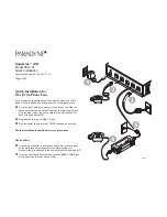
4
4-2
4.3
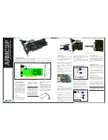
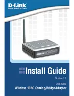
BLOCK DIAGRAM DESCRIPTION
Figure 4-1 shows a block diagram of the N4865A’s internal logic. Most of the
major logic elements center around the 16-bit data bus from the ARM7 Proces-
sor. The N4865A has a LAN Interface, a static 1 Mbyte RAM chip, a FLASH,
a GPIB Interface and a LED Latch chip, all controlled by an ARM7 Processor.
The FLASH chip stores the program code and the confi guration parameters.
At power turn-on time, the ARM7 processor loads the program code from the
FLASH into the RAM chip. The program is then run out of the RAM chip.
At power turn-on, the processor clears the LEDs, does a brief check of the
logic elements and then checks the FLASH to fi nd the correct program. If the
processor had found a hardware error, the loading process would stop and the
LEDs would blink the appropriate error code. New units default to using the
program stored in the program0 space. Units that have been updated in the
fi eld use the program stored in the program1 space. If the code in program1
space is corrupted, the N4865A reverts to the factory installed code in the
program0 space.
Figure 4-1 N4865A Block Diagram
Power
Supply
9-32 VDC
Input
+5V
3.3V
Reg
+3.3V
GPIB
CTLR
RAM
ARM7 Processor
+5
+5
Address
DCDR
µP BUS
FLASH
Latch
Front Panel LEDs
LAN
INTFC
GPIB
Fltr
TCP/IP
LAN
Rear Panel
Reset Button
Summary of Contents for N4865A
Page 20: ...1 16 1 This page left intentionally blank ...
Page 32: ...2 12 2 This page left intentionally blank ...
Page 40: ...3 8 3 This page left intentionally blank ...
Page 44: ...4 4 4 This page purposely left blank ...
Page 96: ...A 44 A2 This page purposely left blank ...
Page 100: ...Index 4 I This page left intentionally blank ...