background image

Rev. 2.10

62

���� 02� 201�

Rev. 2.10 

63

���� 02� 201�

HT68F20/HT68F30/HT68F40/HT68F50/HT68F60

HT68FU30/HT68FU40/HT68FU50/HT68FU60

Enhanced I/O Flash Type 8-Bit MCU with EEPROM

HT68F20/HT68F30/HT68F40/HT68F50/HT68F60

HT68FU30/HT68FU40/HT68FU50/HT68FU60

Enhanced I/O Flash Type 8-Bit MCU with EEPROM

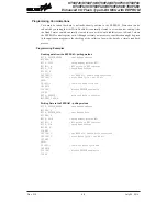
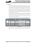
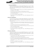
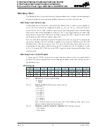
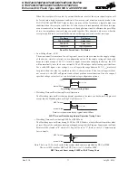
NORMAL Mode to SLOW Mode Switching

When running in the NORMAL Mode, which uses the high speed system oscillator, and therefore 
consumes more power, the system clock can switch to run in the SLOW Mode by set the HLCLK bit 
to "0" and set the CKS2~CKS0 bits to "000" or "001" in the SMOD register. This will then use the 
low speed system oscillator which will consume less power. Users may decide to do this for certain 
operations which do not require high performance and can subsequently reduce power consumption. 
The SLOW Mode is sourced from the LXT or the LIRC oscillators and therefore requires these 
oscillators to be stable before full mode switching occurs. This is monitored using the LTO bit in the 
SMOD register.


                      


            ­            ­     

               


            ­            ­     

          €  ‚  ƒ      

            ­            ­     

          €  ‚  ƒ      

            ­            ­     

Summary of Contents for HT68F30

Page 1: ...Enhanced I O Flash Type 8 Bit MCU with EEPROM HT68F20 HT68F30 HT68F40 HT68F50 HT68F60 HT68FU30 HT68FU40 HT68FU50 HT68FU60 Revision V2 10 Date July 02 2014 ...

Page 2: ...rator Electrical Characteristics 25 Power on Reset Characteristics 25 System Architecture 26 Clocking and Pipelining 26 Program Counter 27 Stack 28 Arithmetic and Logic Unit ALU 28 Flash Program Memory 29 Structure 29 Special Vectors 30 Look up Table 30 Table Program Example 31 In Circuit Programming 32 RAM Data Memory 33 Structure 33 Special Function Register Description 37 Indirect Addressing Re...

Page 3: ...52 External 32 768kHz Crystal Oscillator LXT 53 LXT Oscillator Low Power Function 54 Internal 32kHz Oscillator LIRC 54 Supplementary Oscillators 54 Operating Modes and System Clocks 55 System Clocks 55 System Operation Modes 57 Control Register 58 Fast Wake up 60 Operating Mode Switching and Wake up 61 NORMAL Mode to SLOW Mode Switching 62 SLOW Mode to NORMAL Mode Switching 63 Entering the SLEEP1 ...

Page 4: ...g Considerations 109 Compact Type TM 110 Compact TM Operation 110 Compact Type TM Register Description 111 Compact Type TM Operating Modes 115 Compare Match Output Mode 115 Timer Counter Mode 115 PWM Output Mode 118 Standard Type TM STM 121 Standard TM Operation 121 Standard Type TM Register Description 122 Standard Type TM Operating Modes 131 Compare Output Mode 131 Timer Counter Mode 134 PWM Out...

Page 5: ...ave Address 182 I2 C Bus Read Write Signal 183 I2 C Bus Data and Acknowledge Signal 183 Peripheral Clock Output 185 Peripheral Clock Operation 185 Interrupts 186 Interrupt Registers 186 Interrupt Operation 200 External Interrupt 204 Comparator Interrupt 204 Multi function Interrupt 205 Time Base Interrupts 205 Serial Interface Module Interrupt 207 External Peripheral Interrupt 207 EEPROM Interrupt...

Page 6: ...Module Internal Signal 225 UART Module SPI Interface 225 UART Module External Pin Interfacing 226 UART Data Transfer Scheme 227 UART Commands 227 UART Status and Control Registers 228 Baud Rate Generator 233 UART Module Setup and Control 235 Managing Receiver Errors 240 UART Module Interrupt Structure 241 UART Module Power down and Wake up 242 Using the UART Function 243 Application Circuit with U...

Page 7: ...OP 150mil Outline Dimensions 266 24 pin SKDIP 300mil Outline Dimensions 267 24 pin SOP 300mil Outline Dimensions 269 24 pin SSOP 150mil Outline Dimensions 270 28 pin SKDIP 300mil Outline Dimensions 271 28 pin SOP 300mil Outline Dimensions 272 28 pin SSOP 150mil Outline Dimensions 273 SAW Type 32 pin 5mm 5mm QFN Outline Dimensions 274 SAW Type 40 pin 6mm 6mm for 0 75mm QFN Outline Dimensions 275 44...

Page 8: ...at VDD 5V Power down and wake up functions to reduce power consumption Five oscillators External Crystal HXT External 32 768kHz Crystal LXT External RC ERC Internal RC HIRC Internal 32kHz RC LIRC Multi mode operation NORMAL SLOW IDLE and SLEEP Fully integrated internal 4MHz 8MHz and 12MHz oscillator requires no external components All instructions executed in one or two instruction cycles Table re...

Page 9: ...r Module for time measure input capture compare match output PWM output or single pulse output function Serial Interfaces Module SIM for SPI or I2 C Dual Comparator functions Dual Time Base functions for generation of fixed time interrupt signals Low voltage reset function Low voltage detect function Optional peripheral UART module for fully duplex asynchronous communication Wide range of availabl...

Page 10: ...h as an internal Watchdog Timer Low Voltage Reset and Low Voltage Detector coupled with excellent noise immunity and ESD protection ensure that reliable operation is maintained in hostile electrical environments A full choice of HXT LXT ERC HIRC and LIRC oscillator functions are provided including a fully integrated system oscillator which requires no external components for its implementation The...

Page 11: ...IP NSOP SSOP 20DIP SOP SSOP 24SKDIP SOP SSOP HT68FU30 14 24SKDIP SOP HT68F40 2 2V 5 5V 4K 15 192 8 128 8 42 2 10 bit CTM 1 10 bit ETM 1 16 bit STM 1 8 24 28SKDIP SOP SSOP 44LQFP 32 40QFN 48SSOP QFN HT68FU40 34 40QFN 44LQFP 48SSOP QFN HT68F50 2 2V 5 5V 8K 16 384 8 256 8 42 2 10 bit CTM 2 10 bit ETM 1 16 bit STM 1 8 28SKDIP SOP SSOP 44LQFP 40QFN 48SSOP QFN HT68FU50 34 44LQFP 48QFN HT68F60 2 2V 5 5V ...

Page 12: ...Rev 2 10 12 July 02 2014 HT68F20 HT68F30 HT68F40 HT68F50 HT68F60 HT68FU30 HT68FU40 HT68FU50 HT68FU60 Enhanced I O Flash Type 8 Bit MCU with EEPROM Block Diagram ...

Page 13: ... HT68FU60 Enhanced I O Flash Type 8 Bit MCU with EEPROM Pin Assignment Note 1 Bracketed pin names indicate non default pinout remapping locations 2 If the pin shared pin functions have multiple outputs simultaneously its pin names at the right side of the sign can be used for higher priority ...

Page 14: ...HT68FU50 HT68FU60 Enhanced I O Flash Type 8 Bit MCU with EEPROM Note 1 Bracketed pin names indicate non default pinout remapping locations 2 If the pin shared pin functions have multiple outputs simultaneously its pin names at the right side of the sign can be used for higher priority ...

Page 15: ...HT68FU50 HT68FU60 Enhanced I O Flash Type 8 Bit MCU with EEPROM Note 1 Bracketed pin names indicate non default pinout remapping locations 2 If the pin shared pin functions have multiple outputs simultaneously its pin names at the right side of the sign can be used for higher priority ...

Page 16: ...HT68FU50 HT68FU60 Enhanced I O Flash Type 8 Bit MCU with EEPROM Note 1 Bracketed pin names indicate non default pinout remapping locations 2 If the pin shared pin functions have multiple outputs simultaneously its pin names at the right side of the sign can be used for higher priority ...

Page 17: ...nput CP0C CP1C AN PA3 PC3 C0 C1 Comparator 0 1 input AN PA2 PC2 C0X C1X Comparator 0 1 output CMOS PA0 PA5 TCK0 TCK1 TM0 TM1 input ST PA2 PA4 TP0_0 TM0 I O TMPC0 ST CMOS PA0 TP1_0 TP1_1 TM1 I O TMPC0 ST CMOS PA1 PC0 INT0 INT1 Ext Interrupt 0 1 ST PA3 PA4 PINT Peripheral Interrupt ST PC3 PCK Peripheral Clock output CMOS PC2 SDI SPI Data input ST PA6 SDO SPI Data output CMOS PA5 SCS SPI Slave Select...

Page 18: ...M0 ST PA6 or PC0 SDO SPI Data output PRM0 CMOS PA5 or PC1 SCS SPI Slave Select PRM0 ST CMOS PB5 or PC6 SCK SPI Serial Clock PRM0 ST CMOS PA7 or PC7 SCL I2 C Clock PRM0 ST NMOS PA7 or PC7 SDA I2 C Data PRM0 ST NMOS PA6 or PC0 SCOM0 SCOM3 SCOM0 SCOM3 SCOMC SCOM PC0 PC1 PC6 PC7 OSC1 HXT ERC pin CO HXT PB1 OSC2 HXT pin CO HXT PB2 XT1 LXT pin CO LXT PB3 XT2 LXT pin CO LXT PB4 RES Reset input CO ST PB0 ...

Page 19: ... PINT Peripheral Interrupt PRM0 ST PC3 or PC4 PCK Peripheral Clock output PRM0 CMOS PC2 or PC5 SDI SPI Data input PRM0 ST PA6 or PD2 or PB7 SDO SPI Data output PRM0 CMOS PA5 or PD3 or PB6 SCS SPI Slave Select PRM0 ST CMOS PB5 or PD0 or PD7 SCK SPI Serial Clock PRM0 ST CMOS PA7 or PD1 or PD6 SCL I2 C Clock PRM0 ST NMOS PA7 or PD1 or PD6 SDA I2 C Data PRM0 ST NMOS PA6 or PD2 or PB7 SCOM0 SCOM3 SCOM0...

Page 20: ...T PA3 PA4 or PC4 PC5 or PE6 PE7 PINT Peripheral Interrupt PRM0 ST PC3 or PC4 PCK Peripheral Clock output PRM0 CMOS PC2 or PC5 SDI SPI Data input PRM0 ST PA6 or PD2 or PB7 SDO SPI Data output PRM0 CMOS PA5 or PD3 or PB6 SCS SPI Slave Select PRM0 ST CMOS PB5 or PD0 or PD7 SCK SPI Serial Clock PRM0 ST CMOS PA7 or PD1 or PD6 SCL I2 C Clock PRM0 ST NMOS PA7 or PD1 or PD6 SDA I2 C Data PRM0 ST NMOS PA6 ...

Page 21: ...A3 PA4 PC4 PC5 or PC4 PC5 PE2 or PE0 PE1 or PE6 PE7 PINT Peripheral Interrupt PRM0 ST PC3 or PC4 PCK Peripheral Clock output PRM0 CMOS PC2 or PC5 SDI SPI Data input PRM0 ST PA6 or PD2 or PB7 SDO SPI Data output PRM0 CMOS PA5 or PD3 or PB6 or PD1 SCS SPI Slave Select PRM0 ST CMOS PB5 or PD0 or PD7 SCK SPI Serial Clock PRM0 ST CMOS PA7 or PD1 or PD6 or PD3 SCL I2 C Clock PRM0 ST NMOS PA7 or PD1 or P...

Page 22: ...Hz 4 5 5 5 V IDD1 Operating Current Normal Mode fSYS fH HXT ERC HIRC 3V No load fSYS fH 4MHz WDT enable 0 7 1 1 mA 5V 1 8 2 7 mA 3V No load fSYS fH 8MHz WDT enable 1 6 2 4 mA 5V 3 3 5 0 mA 3V No load fSYS fH 12MHz WDT enable 2 2 3 3 mA 5V 5 0 7 5 mA IDD2 Operating Current Normal Mode fSYS fH HXT 5V No load fSYS fH 20MHz WDT enable 6 0 9 0 mA IDD3 Operating Current Slow Mode fSYS fL LXT LIRC 3V No ...

Page 23: ... 2 70 5 V LVDEN 1 VLVD 3 0V 5 3 00 5 V LVDEN 1 VLVD 3 3V 5 3 30 5 V LVDEN 1 VLVD 3 6V 5 3 60 5 V LVDEN 1 VLVD 4 4V 5 4 4 5 V ILV Additional Power Consumption if LVR and LVD is Used LVR enable LVDEN 0 60 90 μA LVR disable LVDEN 1 75 115 μA LVR enable LVDEN 1 90 135 μA VOL Output Low Voltage I O Port 3V IOL 9mA 0 3 V 5V IOL 20mA 0 5 V VOH Output High Voltage I O Port 3V IOH 3 2mA 2 7 V 5V IOH 7 4mA ...

Page 24: ...12 7 MHz fERC System Clock ERC 5V Ta 25 C R 120kΩ 2 8 2 MHz 5V Ta 0 C 70 C R 120kΩ 5 8 6 MHz 5V Ta 40 C 85 C R 120kΩ 7 8 9 MHz 3 0V 5 5V Ta 40 C 85 C R 120kΩ 9 8 10 MHz 2 2V 5 5V Ta 40 C 85 C R 120kΩ 15 8 10 MHz fLXT System Clock LXT 32 768 kHz fLIRC System Clock LIRC 5V Ta 25 C 10 32 10 kHz 2 2V 5 5V Ta 40 C 85 C 50 32 60 kHz fTIMER Timer Input Pin Frequency 1 fSYS tRES External Reset Low Pulse W...

Page 25: ...teresis Width 20 40 60 mV VCM Comparator Common Mode Voltage Range VSS VDD 1 4V V AOL Comparator Open Loop Gain 60 80 dB tPD Comparator Response Time With 100mV overdrive Note 370 560 ns Note Measured with comparator one input pin at VCM VDD 1 4 2 while the other pin input transition from VSS to VCM 100mV or from VDD to VCM 100mV Power on Reset Characteristics Ta 25 C Symbol Parameter Test Conditi...

Page 26: ...r indirectly addressed The simple addressing methods of these registers along with additional architectural features ensure that a minimum of external components is required to provide a functional I O control system with maximum reliability and flexibility This makes the device suitable for low cost high volume production for controller applications Clocking and Pipelining The main system clock d...

Page 27: ...nstructions requiring jumps to non consecutive addresses such as a jump instruction a subroutine call interrupt or reset etc the microcontroller manages program control by loading the required address into the Program Counter For conditional skip instructions once the condition has been met the next instruction which has already been fetched during the present instruction execution is discarded an...

Page 28: ...ll a CALL subroutine instruction can still be executed which will result in a stack overflow Precautions should be taken to avoid such cases which might cause unpredictable program branching If the stack is overflow the first Program Counter save in the stack will be lost P r o g r a m C o u n t e r S t a c k L e v e l 1 S t a c k L e v e l 2 S t a c k L e v e l 3 S t a c k L e v e l N P r o g r a...

Page 29: ...s to 12K 16 bits The Program Memory is addressed by the Program Counter and also contains data table information and interrupt entries Table data which can be setup in any location within the Program Memory is addressed by a separate table pointer register Device Capacity Banks HT68F20 1K 14 0 HT68F30 2K 14 0 HT68F40 4K 15 0 HT68F50 8K 16 0 HT68F60 12K 16 0 1 The HT68F60 has its Program Memory div...

Page 30: ...able pointer register TBLP and TBHP These registers define the total address of the look up table After setting up the table pointer the table data can be retrieved from the Program Memory using the TABRD m or TABRDL m instructions respectively When the instruction is executed the lower order table byte from the Program Memory will be transferred to the user defined Data Memory register m as speci...

Page 31: ...its protection if both the main routine and Interrupt Service Routine use table read instructions If using the table read instructions the Interrupt Service Routines may change the value of the TBLH and subsequently cause errors if used again by the main routine As a rule it is recommended that simultaneous use of the table read instructions should be avoided However in situations where simultaneo...

Page 32: ...The Program Memory and EEPROM data memory can both be programmed serially in circuit using this 5 wire interface Data is downloaded and uploaded serially on a single pin with an additional line for the clock Two additional lines are required for the power supply and one line for the reset The technical details regarding the in circuit programming of the devices are beyond the scope of this documen...

Page 33: ...is known as the General Purpose Data Memory which is reserved for general purpose use All locations within this area are read and write accessible under program control The overall Data Memory is subdivided into several banks the structure of which depends upon the device chosen The Special Purpose Data Memory registers are accessible in all banks with the exception of the EEC register at address ...

Page 34: ... 34 July 02 2014 HT68F20 HT68F30 HT68F40 HT68F50 HT68F60 HT68FU30 HT68FU40 HT68FU50 HT68FU60 Enhanced I O Flash Type 8 Bit MCU with EEPROM HT68F20 Special Purpose Data Memory HT68F30 Special Purpose Data Memory ...

Page 35: ... 35 July 02 2014 HT68F20 HT68F30 HT68F40 HT68F50 HT68F60 HT68FU30 HT68FU40 HT68FU50 HT68FU60 Enhanced I O Flash Type 8 Bit MCU with EEPROM HT68F40 Special Purpose Data Memory HT68F50 Special Purpose Data Memory ...

Page 36: ...Rev 2 10 36 July 02 2014 HT68F20 HT68F30 HT68F40 HT68F50 HT68F60 HT68FU30 HT68FU40 HT68FU50 HT68FU60 Enhanced I O Flash Type 8 Bit MCU with EEPROM HT68F60 Special Purpose Data Memory ...

Page 37: ...Indirect Addressing Registers are not physically implemented reading the Indirect Addressing Registers indirectly will return a result of 00H and writing to the registers indirectly will result in no operation Memory Pointers MP0 MP1 Two Memory Pointers known as MP0 and MP1 are provided These Memory Pointers are physically implemented in the Data Memory and can be manipulated in the same way as no...

Page 38: ...al banks Selecting the required Program and Data Memory area is achieved using the Bank Pointer Bit 5 of the Bank Pointer is used to select Program Memory Bank 0 or 1 while bits 0 2 are used to select Data Memory Banks 0 4 The Data Memory is initialised to Bank 0 after a reset except for a WDT time out reset in the Power Down Mode in which case the Data Memory bank remains unaffected It should be ...

Page 39: ...BP0 R W R W R W POR 0 0 Bit 7 2 Unimplemented read as 0 Bit 1 0 DMBP1 DMBP0 Select Data Memory Banks 00 Bank 0 01 Bank 1 10 Bank 2 11 Undefined HT68F60 Bit 7 6 5 4 3 2 1 0 Name PMBP0 DMBP2 DMBP1 DMBP0 R W R W R W R W R W POR 0 0 0 0 Bit 7 6 Unimplemented read as 0 Bit 5 PMBP0 Select Program Memory Banks 0 Bank 0 Program Memory Address is from 0000H 1FFFH 1 Bank 1 Program Memory Address is from 200...

Page 40: ...e low byte of the Program Counter is made accessible to programmers by locating it within the Special Purpose area of the Data Memory By manipulating this register direct jumps to other program locations are easily implemented Loading a value directly into this PCL register will cause a jump to the specified Program Memory location however as the register is only 8 bit wide only jumps within the c...

Page 41: ...gs generally reflect the status of the latest operations C is set if an operation results in a carry during an addition operation or if a borrow does not take place during a subtraction operation otherwise C is cleared C is also affected by a rotate through carry instruction AC is set if an operation results in a carry out of the low nibbles in addition or no borrow from the high nibble into the l...

Page 42: ...struction Bit 3 OV Overflow flag 0 No overflow 1 An operation results in a carry into the highest order bit but not a carry out of the highest order bit or vice versa Bit 2 Z Zero flag 0 The result of an arithmetic or logical operation is not zero 1 The result of an arithmetic or logical operation is zero Bit 1 AC Auxiliary flag 0 No auxiliary carry 1 An operation results in a carry out of the low...

Page 43: ...mory and RAM Data Memory the EEPROM Data Memory is not directly mapped into memory space and is therefore not directly addressable in the same way as the other types of memory Read and Write operations to the EEPROM are carried out in single byte operations using an address and data register in Bank 0 and a single control register in Bank 1 Device Capacity Address HT68F20 32 8 00H 1FH HT68F30 64 8...

Page 44: ... 1 0 EEA D4 D3 D2 D1 D0 EED D7 D6 D5 D4 D3 D2 D1 D0 EEC WREN WR RDEN RD HT68F30 Name Bit 7 6 5 4 3 2 1 0 EEA D5 D4 D3 D2 D1 D0 EED D7 D6 D5 D4 D3 D2 D1 D0 EEC WREN WR RDEN RD HT68F40 Name Bit 7 6 5 4 3 2 1 0 EEA D6 D5 D4 D3 D2 D1 D0 EED D7 D6 D5 D4 D3 D2 D1 D0 EEC WREN WR RDEN RD HT68F50 HT68F60 Name Bit 7 6 5 4 3 2 1 0 EEA D7 D6 D5 D4 D3 D2 D1 D0 EED D7 D6 D5 D4 D3 D2 D1 D0 EEC WREN WR RDEN RD ...

Page 45: ...8F30 Bit 7 6 5 4 3 2 1 0 Name D5 D4 D3 D2 D1 D0 R W R W R W R W R W R W R W POR unknown Bit 7 6 Unimplemented read as 0 Bit 5 0 Data EEPROM address Data EEPROM address bit 5 bit 0 HT68F40 Bit 7 6 5 4 3 2 1 0 Name D6 D5 D4 D3 D2 D1 D0 R W R W R W R W R W R W R W R W POR unknown Bit 7 Unimplemented read as 0 Bit 6 0 Data EEPROM address Data EEPROM address bit 6 bit 0 HT68F50 HT68F60 Bit 7 6 5 4 3 2 ...

Page 46: ...it will be automatically reset to zero by the hardware after the write cycle has finished Setting this bit high will have no effect if the WREN has not first been set high Bit 1 RDEN Data EEPROM Read Enable 0 Disable 1 Enable This is the Data EEPROM Read Enable Bit which must be set high before Data EEPROM read operations are carried out Clearing this bit to zero will inhibit Data EEPROM read oper...

Page 47: ...her by polling the WR bit in the EEC register or by using the EEPROM interrupt When the write cycle terminates the WR bit will be automatically cleared to zero by the microcontroller informing the user that the data has been written to the EEPROM The application program can therefore poll the WR bit to determine when the write cycle has ended Write Protection Protection against inadvertent write o...

Page 48: ...Reading data from the EEPROM polling method MOV A EEPROM_ADRES user defined address MOV EEA A MOV A 040H setup memory pointer MP1 MOV MP1 A MP1 points to EEC register MOV A 01H setup Bank Pointer MOV BP A SET IAR1 1 set RDEN bit enable read operations SET IAR1 0 start Read Cycle set RD bit BACK SZ IAR1 0 check for read cycle end JMP BACK CLR IAR1 disable EEPROM read write CLR BP MOV A EEDATA move ...

Page 49: ...the device has the flexibility to optimize the performance power ratio a feature especially important in power sensitive portable applications Type Name Freq Pins External Crystal HXT 400kHz 20MHz OSC1 OSC2 External RC ERC 8MHz OSC1 Internal High Speed RC HIRC 4 8 or 12MHz External Low Speed Crystal LXT 32 768kHz XT1 XT2 Internal Low Speed RC LIRC 32kHz Oscillator Types System Clock Configurations...

Page 50: ...Rev 2 10 50 July 02 2014 HT68F20 HT68F30 HT68F40 HT68F50 HT68F60 HT68FU30 HT68FU40 HT68FU50 HT68FU60 Enhanced I O Flash Type 8 Bit MCU with EEPROM System Clock Configurations ...

Page 51: ...tion it may be necessary to add two small value capacitors C1 and C2 Using a ceramic resonator will usually require two small value capacitors C1 and C2 to be connected as shown for oscillation to occur The values of C1 and C2 should be selected in consultation with the crystal or resonator manufacturer s specification For oscillator stability and to minimise the effects of noise and crosstalk it ...

Page 52: ... of 25 C degrees the oscillator will have a frequency of 8MHz within a tolerance of 2 Here only the OSC1 pin is used which is shared with I O pin PB1 leaving pin PB2 free for use as a normal I O pin For oscillator stability and to minimise the effects of noise and crosstalk it is important to locate the capacitor and resistoras close to the MCU as possible External RC Oscillator ERC Internal RC Os...

Page 53: ...nternal timers operational even when the microcontroller is in the SLEEP or IDLE Mode To do this another clock independent of the system clock must be provided However for some crystals to ensure oscillation and accurate frequency generation it is necessary to add two small value external capacitors C1 and C2 The exact values of C1 and C2 should be selected in consultation with the crystal or reso...

Page 54: ...commended that the application program sets the LXTLP bit high about 2 seconds after power on It should be noted that no matter what condition the LXTLP bit is set to the LXT oscillator will always function normally the only difference is that it will take more time to start up if in the Low power mode Internal 32kHz Oscillator LIRC The Internal 32kHz System Oscillator is one of the low frequency ...

Page 55: ...ster programming a clock system can be configured to obtain maximum application performance The main system clock can come from either a high frequency fH or low frequency fL source and is selected using the HLCLK bit and CKS2 CKS0 bits in the SMOD register The high speed system clock can be sourced from either an HXT ERC or HIRC oscillator selected via a configuration option The low speed system ...

Page 56: ...68FU40 HT68FU50 HT68FU60 Enhanced I O Flash Type 8 Bit MCU with EEPROM System Clock Configurations Note When the system clock source fSYS is switched to fL from fH the high speed oscillation will stop to conserve the power Thus there is no fH fH 64 for peripheral circuit to use ...

Page 57: ...s either the HXT ERC or HIRC oscillators The high speed oscillator will however first be divided by a ratio ranging from 1 to 64 the actual ratio being selected by the CKS2 CKS0 and HLCLK bits in the SMOD register Although a high speed oscillator is used running the microcontroller at a divided clock ratio reduces the operating current SLOW Mode This is also a mode where the microcontroller operat...

Page 58: ...tchdog Timer TMs and SIM In the IDLE1 Mode the system oscillator will continue to run and this system oscillator may be high speed or low speed system oscillator In the IDLE1 Mode the Watchdog Timer clock fS will be on If the source is fSYS 4 then the fS clock will be on and if the source comes from fSUB then fS will be on Control Register A single register SMOD is used for overall control of the ...

Page 59: ... device power on The flag will be low when in the SLEEP or IDLE0 Mode but after a wake up has occurred the flag will change to a high level after 1024 clock cycles if the HXT oscillator is used and after 15 16 clock cycles if the ERC or HIRC oscillator is used Bit 1 IDLEN IDLE Mode control 0 Disable 1 Enable This is the IDLE Mode Control bit and determines what happens when the HALT instruction is...

Page 60: ...unction is enabled then it will take one to two tSUB clock cycles of the LIRC or LXT oscillator for the system to wake up The system will then initially run under the fSUB clock source until 1024 HXT clock cycles have elapsed at which point the HTO flag will switch high and the system will switch over to operating from the HXT oscillator If the ERC or HIRC oscillators or LIRC oscillator is used as...

Page 61: ...MOD register while Mode Switching from the NORMAL SLOW Modes to the SLEEP IDLE Modes is executed via the HALT instruction When a HALT instruction is executed whether the device enters the IDLE Mode or the SLEEP Mode is determined by the condition of the IDLEN bit in the SMOD register and FSYSON in the WDTC register When the HLCLK bit switches to a low level which implies that clock source is switc...

Page 62: ... in the SLOW Mode by set the HLCLK bit to 0 and set the CKS2 CKS0 bits to 000 or 001 in the SMOD register This will then use the low speed system oscillator which will consume less power Users may decide to do this for certain operations which do not require high performance and can subsequently reduce power consumption The SLOW Mode is sourced from the LXT or the LIRC oscillators and therefore re...

Page 63: ...oscillator To switch back to the NORMAL Mode where the high speed system oscillator is used the HLCLK bit should be set to 1 or HLCLK bit is 0 but CKS2 CKS0 is set to 010 011 100 101 110 or 111 As a certain amount of time will be required for the high frequency clock to stabilise the status of the HTO bit is checked The amount of time required for high speed system oscillator stabilization depends...

Page 64: ...e system clock and Time Base clock will be stopped and the application program will stop at the HALT instruction but the WDT or LVD will remain with the clock source coming from the fSUB clock The Data Memory contents and registers will maintain their present condition The WDT will be cleared and resume counting if the WDT clock source is selected to come from the fSUB clock as the WDT is enabled ...

Page 65: ... the current consumption of the device to as low a value as possible perhaps only in the order of several micro amps except in the IDLE1 Mode there are other considerations which must also be taken into account by the circuit designer if the power consumption is to be minimised Special attention must be made to the I O pins on the device All high impedance input pins must be connected to either a ...

Page 66: ...is situation the interrupt which woke up the device will not be immediately serviced but will rather be serviced later when the related interrupt is finally enabled or when a stack level becomes free The other situation is where the related interrupt is enabled and the stack is not full in which case the regular interrupt response takes place If an interrupt request flag is set high before enterin...

Page 67: ...rature and process variations The LXT oscillator is supplied by an external 32 768kHz crystal The other Watchdog Timer clock source option is the fSYS 4 clock The Watchdog Timer clock source can originate from its own internal LIRC oscillator the LXT oscillator or fSYS 4 It is divided by a value of 28 to 215 using the WS2 WS0 bits in the WDTC register to obtain the required Watchdog Timer time out...

Page 68: ...Enable Disable Control Under normal program operation a Watchdog Timer time out will initialise a device reset and set the status bit TO However if the system is in the SLEEP or IDLE Mode when a Watchdog Timer time out occurs the TO bit in the status register will be set and only the Program Counter and Stack Pointer will be reset Three methods can be adopted to clear the contents of the Watchdog ...

Page 69: ...and the microcontroller is already running the RES line is forcefully pulled low In such a case known as a normal operation reset some of the microcontroller registers remain unchanged allowing the microcontroller to proceed with normal operation after the reset line is allowed to return high Another type of reset is when the Watchdog Timer overflows and resets the microcontroller All types of res...

Page 70: ...ich the microcontroller will begin normal operation The abbreviation SST in the figures stands for System Start up Timer For most applications a resistor connected between VDD and the RES pin and a capacitor connected between VSS and the RES pin will provide a suitable external reset circuit Any wiring connected to the RES pin should be kept as short as possible to minimise any stray noise interfe...

Page 71: ...en changing the battery the LVR will automatically reset the device internally The LVR includes the following specifications For a valid LVR signal a low voltage i e a voltage in the range between 0 9V VLVR must exist for greater than the value tLVR specified in the A C characteristics If the low voltage state does not exceed tLVR the LVR will ignore it and will not perform a reset function One of...

Page 72: ...l registers of the microcontroller in different ways To ensure reliable continuation of normal program execution after a reset occurs it is important to know what condition the microcontroller is in after a particular reset occurs The following table describes how each type of reset affects each of the microcontroller internal registers Note that where more than one package type exists the table w...

Page 73: ... 0 1 1 0 0 0 0 0 0 1 1 0 0 0 0 0 0 1 uuuu uuuu SIMD x x x x x x x x x x x x x x x x x x x x x x x x uuuu uuuu SIMA SIMC2 0 0 0 0 0 0 0 0 0 0 0 0 0 0 0 0 0 0 0 0 0 0 0 0 uuuu uuuu TM0C0 0 0 0 0 0 0 0 0 0 0 0 0 0 0 0 0 0 0 0 0 0 0 0 0 uuuu uuuu TM0C1 0 0 0 0 0 0 0 0 0 0 0 0 0 0 0 0 0 0 0 0 0 0 0 0 uuuu uuuu TM0DL 0 0 0 0 0 0 0 0 0 0 0 0 0 0 0 0 0 0 0 0 0 0 0 0 uuuu uuuu TM0DH 00 00 00 uu TM0AL 0 0 0...

Page 74: ...000 000 0 0 0 0 0 0 uuu uuu MFI2 0 0 0 0 0 0 0 0 0 0 0 0 0 0 0 0 0 0 0 0 0 0 0 0 uuuu uuuu PAWU 0 0 0 0 0 0 0 0 0 0 0 0 0 0 0 0 0 0 0 0 0 0 0 0 uuuu uuuu PAPU 0 0 0 0 0 0 0 0 0 0 0 0 0 0 0 0 0 0 0 0 0 0 0 0 uuuu uuuu PA 1111 1111 1111 1111 1111 1111 uuuu uuuu PAC 1111 1111 1111 1111 1111 1111 uuuu uuuu PBPU 00 0000 00 0000 00 0000 uu uuuu PB 11 1111 11 1111 11 1111 uu uuuu PBC 11 1111 11 1111 11 1...

Page 75: ... 0 0 0 0 0 0 0 uuuu uuuu TM1C1 0 0 0 0 0 0 0 0 0 0 0 0 0 0 0 0 0 0 0 0 0 0 0 0 uuuu uuuu TM1C2 0 0 0 0 0 0 0 0 0 0 0 0 0 0 0 0 0 0 0 0 0 0 0 0 uuuu uuuu TM1DL 0 0 0 0 0 0 0 0 0 0 0 0 0 0 0 0 0 0 0 0 0 0 0 0 uuuu uuuu TM1DH 00 00 00 uu TM1AL 0 0 0 0 0 0 0 0 0 0 0 0 0 0 0 0 0 0 0 0 0 0 0 0 uuuu uuuu TM1AH 00 00 00 uu TM1BL 0 0 0 0 0 0 0 0 0 0 0 0 0 0 0 0 0 0 0 0 0 0 0 0 uuuu uuuu TM1BH 00 00 00 uu S...

Page 76: ...00 000 000 000 uuu uuu MFI2 0 0 0 0 0 0 0 0 0 0 0 0 0 0 0 0 0 0 0 0 0 0 0 0 uuuu uuuu PAWU 0 0 0 0 0 0 0 0 0 0 0 0 0 0 0 0 0 0 0 0 0 0 0 0 uuuu uuuu PAPU 0 0 0 0 0 0 0 0 0 0 0 0 0 0 0 0 0 0 0 0 0 0 0 0 uuuu uuuu PA 1111 1111 1111 1111 1111 1111 uuuu uuuu PAC 1111 1111 1111 1111 1111 1111 uuuu uuuu PBPU 0 0 0 0 0 0 0 0 0 0 0 0 0 0 0 0 0 0 0 0 0 0 0 0 uuuu uuuu PB 1111 1111 1111 1111 1111 1111 uuuu ...

Page 77: ...TM1C0 0 0 0 0 0 0 0 0 0 0 0 0 0 0 0 0 0 0 0 0 0 0 0 0 uuuu uuuu TM1C1 0 0 0 0 0 0 0 0 0 0 0 0 0 0 0 0 0 0 0 0 0 0 0 0 uuuu uuuu TM1C2 0 0 0 0 0 0 0 0 0 0 0 0 0 0 0 0 0 0 0 0 0 0 0 0 uuuu uuuu TM1DL 0 0 0 0 0 0 0 0 0 0 0 0 0 0 0 0 0 0 0 0 0 0 0 0 uuuu uuuu TM1DH 00 00 00 uu TM1AL 0 0 0 0 0 0 0 0 0 0 0 0 0 0 0 0 0 0 0 0 0 0 0 0 uuuu uuuu TM1AH 00 00 00 uu TM1BL 0 0 0 0 0 0 0 0 0 0 0 0 0 0 0 0 0 0 0 ...

Page 78: ... uuuu uuuu MFI1 000 000 000 000 000 000 uuu uuu MFI2 0 0 0 0 0 0 0 0 0 0 0 0 0 0 0 0 0 0 0 0 0 0 0 0 uuuu uuuu MFI3 0 0 0 0 0 0 0 0 0 0 0 0 uu uu PAWU 0 0 0 0 0 0 0 0 0 0 0 0 0 0 0 0 0 0 0 0 0 0 0 0 uuuu uuuu PAPU 0 0 0 0 0 0 0 0 0 0 0 0 0 0 0 0 0 0 0 0 0 0 0 0 uuuu uuuu PA 1111 1111 1111 1111 1111 1111 uuuu uuuu PAC 1111 1111 1111 1111 1111 1111 uuuu uuuu PBPU 0 0 0 0 0 0 0 0 0 0 0 0 0 0 0 0 0 0 ...

Page 79: ... 0 0 0 0 0 0 0 0 0 0 uuuu uuuu TM1C2 0 0 0 0 0 0 0 0 0 0 0 0 0 0 0 0 0 0 0 0 0 0 0 0 uuuu uuuu TM1DL 0 0 0 0 0 0 0 0 0 0 0 0 0 0 0 0 0 0 0 0 0 0 0 0 uuuu uuuu TM1DH 00 00 00 uu TM1AL 0 0 0 0 0 0 0 0 0 0 0 0 0 0 0 0 0 0 0 0 0 0 0 0 uuuu uuuu TM1AH 00 00 00 uu TM1BL 0 0 0 0 0 0 0 0 0 0 0 0 0 0 0 0 0 0 0 0 0 0 0 0 uuuu uuuu TM1BH 00 00 00 uu TM2C0 0000 0 0000 0 0000 0 uuuu u TM2C1 0 0 0 0 0 0 0 0 0 0...

Page 80: ...0 0 0 0 0 0 0 0 0 0 0 0 0 0 0 0 0 0 0 0 0 0 uuuu uuuu MFI0 0 0 0 0 0 0 0 0 0 0 0 0 0 0 0 0 0 0 0 0 0 0 0 0 uuuu uuuu MFI1 000 000 000 000 000 000 uuu uuu MFI2 0 0 0 0 0 0 0 0 0 0 0 0 0 0 0 0 0 0 0 0 0 0 0 0 uuuu uuuu MFI3 0 0 0 0 0 0 0 0 0 0 0 0 uu uu PAWU 0 0 0 0 0 0 0 0 0 0 0 0 0 0 0 0 0 0 0 0 0 0 0 0 uuuu uuuu PAPU 0 0 0 0 0 0 0 0 0 0 0 0 0 0 0 0 0 0 0 0 0 0 0 0 uuuu uuuu PA 1111 1111 1111 1111...

Page 81: ...0 0 0 0 0 0 0 0 0 0 0 0 0 0 0 0 0 0 0 uuuu uuuu TM1C0 0 0 0 0 0 0 0 0 0 0 0 0 0 0 0 0 0 0 0 0 0 0 0 0 uuuu uuuu TM1C1 0 0 0 0 0 0 0 0 0 0 0 0 0 0 0 0 0 0 0 0 0 0 0 0 uuuu uuuu TM1C2 0 0 0 0 0 0 0 0 0 0 0 0 0 0 0 0 0 0 0 0 0 0 0 0 uuuu uuuu TM1DL 0 0 0 0 0 0 0 0 0 0 0 0 0 0 0 0 0 0 0 0 0 0 0 0 uuuu uuuu TM1DH 00 00 00 uu TM1AL 0 0 0 0 0 0 0 0 0 0 0 0 0 0 0 0 0 0 0 0 0 0 0 0 uuuu uuuu TM1AH 00 00 00...

Page 82: ...these I O ports can be used for input and output operations For input operation these ports are non latching which means the inputs must be ready at the T2 rising edge of instruction MOV A m where m denotes the port address For output operation all the data is latched and remains unchanged until the output latch is rewritten I O Register List HT68F20 Register Name Bit 7 6 5 4 3 2 1 0 PAWU D7 D6 D5...

Page 83: ...7 D6 D5 D4 D3 D2 D1 D0 PEPU D7 D6 D5 D4 D3 D2 D1 D0 PE D7 D6 D5 D4 D3 D2 D1 D0 PEC D7 D6 D5 D4 D3 D2 D1 D0 PFPU D1 D0 PF D1 D0 PFC D1 D0 HT68F60 Register Name Bit 7 6 5 4 3 2 1 0 PAWU D7 D6 D5 D4 D3 D2 D1 D0 PAPU D7 D6 D5 D4 D3 D2 D1 D0 PA D7 D6 D5 D4 D3 D2 D1 D0 PAC D7 D6 D5 D4 D3 D2 D1 D0 PBPU D7 D6 D5 D4 D3 D2 D1 D0 PB D7 D6 D5 D4 D3 D2 D1 D0 PBC D7 D6 D5 D4 D3 D2 D1 D0 PCPU D7 D6 D5 D4 D3 D2 D...

Page 84: ...plemented using weak PMOS transistors PAPU Register Bit 7 6 5 4 3 2 1 0 Name D7 D6 D5 D4 D3 D2 D1 D0 R W R W R W R W R W R W R W R W R W POR 0 0 0 0 0 0 0 0 PBPU Register HT68F40 HT68F50 HT68F60 Bit 7 6 5 4 3 2 1 0 Name D7 D6 D5 D4 D3 D2 D1 D0 R W R W R W R W R W R W R W R W R W POR 0 0 0 0 0 0 0 0 PCPU Register HT68F30 HT68F40 HT68F50 HT68F60 Bit 7 6 5 4 3 2 1 0 Name D7 D6 D5 D4 D3 D2 D1 D0 R W R...

Page 85: ...8F30 Bit 7 6 5 4 3 2 1 0 Name D5 D4 D3 D2 D1 D0 R W R W R W R W R W R W R W POR 0 0 0 0 0 0 Bit 7 6 Unimplemented read as 0 Bit 5 0 PBPU Port B bit 5 bit 0 Pull High Control 0 Disable 1 Enable PCPU Register HT68F20 Bit 7 6 5 4 3 2 1 0 Name D3 D2 D1 D0 R W R W R W R W R W POR 0 0 0 0 Bit 7 4 Unimplemented read as 0 Bit 3 0 PCPU Port C bit 3 bit 0 Pull High Control 0 Disable 1 Enable PFPU Register H...

Page 86: ... W R W R W R W R W R W POR 0 0 0 0 0 0 0 0 Bit 7 0 PAWU Port A bit 7 bit 0 Wake up Control 0 Disable 1 Enable I O Port Control Registers Each I O port has its own control register known as PAC PGC to control the input output configuration With this control register each CMOS output or input can be reconfigured dynamically under software control Each pin of the I O ports is directly mapped to a bit...

Page 87: ...e D7 D6 D5 D4 D3 D2 D1 D0 R W R W R W R W R W R W R W R W R W POR 1 1 1 1 1 1 1 1 PDC Register HT68F40 HT68F50 HT68F60 Bit 7 6 5 4 3 2 1 0 Name D7 D6 D5 D4 D3 D2 D1 D0 R W R W R W R W R W R W R W R W R W POR 1 1 1 1 1 1 1 1 PEC Register HT68F40 HT68F50 HT68F60 Bit 7 6 5 4 3 2 1 0 Name D7 D6 D5 D4 D3 D2 D1 D0 R W R W R W R W R W R W R W R W R W POR 1 1 1 1 1 1 1 1 PFC Register HT68F60 Bit 7 6 5 4 3...

Page 88: ...ut 1 Input PCC Register HT68F20 Bit 7 6 5 4 3 2 1 0 Name D3 D2 D1 D0 R W R W R W R W R W POR 0 0 0 0 Bit 7 4 Unimplemented read as 0 Bit 3 0 PCC Port C bit 3 bit 0 Input Output Control 0 Output 1 Input PFC Register HT68F40 HT68F50 Bit 7 6 5 4 3 2 1 0 Name D1 D0 R W R W R W POR 0 0 Bit 7 2 Unimplemented read as 0 Bit 1 0 PFC Port F bit 1 bit 0 Input Output Control 0 Output 1 Input PGC Register HT68...

Page 89: ... certain device can contain However by allowing the same pins to share several different functions and providing a means of function selection a wide range of different functions can be incorporated into even relatively small package sizes Some devices include PRM0 PRM1 or PRM2 registers which can select the functions of certain pins Pin remapping Register List HT68F30 Register Name Bit 7 6 5 4 3 ...

Page 90: ...PC4 PRM0 Register HT68F40 HT68F50 Bit 7 6 5 4 3 2 1 0 Name C1XPS0 C0XPS0 PDPRM SIMPS1 SIMPS0 PCKPS R W R W R W R W R W R W R W POR 0 0 0 0 0 0 Bit 7 Unimplemented read as 0 Bit 6 C1XPS0 C1X Pin Remapping Control 0 C1X on PA5 1 C1X on PF1 Bit 5 Unimplemented read as 0 Bit 4 C0XPS0 C0X Pin Remapping Control 0 C0X on PA0 1 C0X on PF0 Bit 3 PDPRM PD3 PD0 pin shared function Pin Remapping Control 0 No ...

Page 91: ...apping Control 00 C0X on PA0 01 C0X on PF0 10 C0X on PG0 11 Undefined Bit 3 PDPRM PD3 PD0 pin shared function Pin Remapping Control 0 No change 1 TCK2 on PD0 change to PB6 TP2_0 on PD1 change to PB7 TCK0 on PD2 change to PD6 TCK1 on PD3 change to PD7 if SIMPS1 SIMPS0 01 or 11 Bit 2 1 SIMPS1 SIMPS0 SIM Pin Remapping Control 00 SDO on PA5 SDI SDA on PA6 SCK SCL on PA7 SCS on PB5 01 SDO on PD3 SDI SD...

Page 92: ...W R W R W POR 0 0 0 0 0 0 0 Bit 7 TCK2PS TCK2 Pin Remapping Control 0 TCK2 on PC2 1 TCK2 on PD0 Bit 6 TCK1PS TCK1 Pin Remapping Control 0 TCK1 on PA4 1 TCK1 on PD3 Bit 5 TCK0PS TCK0 Pin Remapping Control 0 TCK0 on PA2 1 TCK0 on PD2 Bit 4 Unimplemented read as 0 Bit 3 2 INT1PS1 INT1PS0 INT1 Pin Remapping Control 00 INT1 on PA4 01 INT1 on PC5 10 Undefined 11 INT1 on PE7 Bit 1 0 INT0PS1 INT0PS0 INT0 ...

Page 93: ... 0 0 0 0 Bit 7 TCK2PS TCK2 Pin Remapping Control 0 TCK2 on PC2 1 TCK2 on PD0 Bit 6 TCK1PS TCK1 Pin Remapping Control 0 TCK1 on PA4 1 TCK1 on PD3 Bit 5 TCK0PS TCK0 Pin Remapping Control 0 TCK0 on PA2 1 TCK0 on PD2 Bit 4 INT2PS INT2 Pin Remapping Control 0 INT2 on PC4 1 INT2 on PE2 Bit 3 2 INT1PS1 INT1PS0 INT1 Pin Remapping Control 00 INT1 on PA4 01 INT1 on PC5 10 INT1 on PE1 11 INT1 on PE7 Bit 1 0 ...

Page 94: ...0 0 0 0 0 0 Bit 7 6 Unimplemented read as 0 Bit 5 TP21PS TP2_1 Pin Remapping Control 0 TP2_1 on PC4 1 TP2_1 on PD4 Bit 4 TP20PS TP2_0 Pin Remapping Control 0 TP2_0 on PC3 1 TP2_0 on PD1 Bit 3 TP1B2PS TP1B_2 Pin Remapping Control 0 TP1B_2 on PC5 1 TP1B_2 on PE4 Bit 2 TP1APS TP1A Pin Remapping Control 0 TP1A on PA1 1 TP1A on PC7 Bit 1 TP01PS TP0_1 Pin Remapping Control 0 TP0_1 on PC5 1 TP0_1 on PD5 ...

Page 95: ...apping Control 0 TP3_1 on PD0 1 TP3_1 on PE3 Bit 6 TP30PS TP3_0 Pin Remapping Control 0 TP3_0 on PD3 1 TP3_0 on PE5 Bit 5 TP21PS TP2_1 Pin Remapping Control 0 TP2_1 on PC4 1 TP2_1 on PD4 Bit 4 TP20PS TP2_0 Pin Remapping Control 0 TP2_0 on PC3 1 TP2_0 on PD1 Bit 3 TP1B2PS TP1B_2 Pin Remapping Control 0 TP1B_2 on PC5 1 TP1B_2 on PE4 Bit 2 TP1APS TP1A Pin Remapping Control 0 TP1A on PA1 1 TP1A on PC7...

Page 96: ...hosen If the port control registers PAC PGC are then programmed to setup some pins as outputs these output pins will have an initial high output value unless the associated port data registers PA PG are first programmed Selecting which pins are inputs and which are outputs can be achieved byte wide by loading the correct values into the appropriate port control register or by programming individua...

Page 97: ... selected with each TM having a reference name of TM0 TM1 TM2 and TM3 Each individual TM can be categorised as a certain type namely Compact Type TM Standard Type TM or Enhanced Type TM Although similar in nature the different TM types vary in their feature complexity The common features to all of the Compact Standard and Enhanced TMs will be described in this section the detailed operation regard...

Page 98: ...pt when a compare match condition occurs As the Enhanced type TM has three internal comparators and comparator A or comparator B or comparator P compare match functions it consequently has three internal interrupts When a TM interrupt is generated it can be used to clear the counter and also to change the state of the TM output pin TM External Pins Each of the TMs irrespective of what type has one...

Page 99: ... TP1B_2 TMPC0 TMPC1 TM Output Pins TM Input Output Pin Control Registers Selecting to have a TM input output or whether to retain its other shared function is implemented using one or two registers with a single bit in each register corresponding to a TM input output pin Setting the bit high will setup the corresponding pin as a TM input output if reset to zero the pin will retain its original oth...

Page 100: ... HT68FU50 HT68FU60 Enhanced I O Flash Type 8 Bit MCU with EEPROM HT68F20 TM Function Pin Control Block Diagram Note The I O register data bits shown are used for TM output inversion control In the Capture Input Mode the TM pin control register must never enable more than one TM input ...

Page 101: ... 1 0 T 1 A C P 0 P A 0 O u t p u t F u n c t i o n 0 1 P A 0 1 0 P A 0 T P 0 _ 0 T 0 C P 0 P C 1 O u t p u t F u n c t i o n 0 1 P C 1 1 0 C C R B O u t p u t C C R B C a p t u r e I n p u t P A 4 T C K 1 T C K I n p u t 1 0 P C 1 T P 1 B _ 1 T 1 B C P 1 T 1 B C P 1 P C 0 O u t p u t F u n c t i o n 0 1 P C 0 1 0 1 0 P C 0 T P 1 B _ 0 T 1 B C P 0 T 1 B C P 0 HT68F30 TM Function Pin Control Block D...

Page 102: ... P A 0 1 0 P A 0 T P 0 _ 0 T 0 C P 0 P C 4 O u t p u t F u n c t i o n 0 1 P C 4 1 0 O u t p u t C a p t u r e I n p u t P C 2 T C K 2 T C K I n p u t 1 0 P C 4 T P 2 _ 1 T 2 C P 1 T 2 C P 1 P C 3 O u t p u t F u n c t i o n 0 1 P C 3 1 0 1 0 P C 3 T P 2 _ 0 T 2 C P 0 T 2 C P 0 HT68F40 TM0 TM2 Function Pin Control Block Diagram Note The I O register data bits shown are used for TM output inversion...

Page 103: ... R B O u t p u t C C R B C a p t u r e I n p u t P A 4 T C K 1 T C K I n p u t 1 0 P C 5 T P 1 B _ 2 T 1 B C P 2 T 1 B C P 2 P C 1 O u t p u t F u n c t i o n 0 1 P C 1 1 0 1 0 P C 1 T P 1 B _ 1 T 1 B C P 1 T 1 B C P 1 P C 0 O u t p u t F u n c t i o n 0 1 P C 0 1 0 P C 0 T P 1 B _ 0 T 1 B C P 0 1 0 T 1 B C P 0 HT68F40 TM1 Function Pin Control Block Diagram Note The I O register data bits shown ar...

Page 104: ...t u r e I n p u t P C 2 T C K 2 T C K I n p u t 1 0 P C 4 T P 2 _ 1 T 2 C P 1 T 2 C P 1 P C 3 O u t p u t F u n c t i o n 0 1 P C 3 1 0 1 0 P C 3 T P 2 _ 0 T 2 C P 0 T 2 C P 0 T C K I n p u t P C 4 T C K 3 P D 0 O u t p u t F u n c t i o n 0 1 P D 0 1 0 O u t p u t P D 0 T P 3 _ 1 T 3 C P 1 P D 3 O u t p u t F u n c t i o n 0 1 P D 3 1 0 P D 3 T P 3 _ 0 T 3 C P 0 HT68F50 and HT68F60 TM0 TM2 TM3 Fu...

Page 105: ... u t p u t C C R B C a p t u r e I n p u t P A 4 T C K 1 T C K I n p u t 1 0 P C 5 T P 1 B _ 2 T 1 B C P 2 T 1 B C P 2 P C 1 O u t p u t F u n c t i o n 0 1 P C 1 1 0 1 0 P C 1 T P 1 B _ 1 T 1 B C P 1 T 1 B C P 1 P C 0 O u t p u t F u n c t i o n 0 1 P C 0 1 0 P C 0 T P 1 B _ 0 T 1 B C P 0 1 0 T 1 B C P 0 HT68F50 and HT68F60 TM1 Function Pin Control Block Diagram Note The I O register data bits sh...

Page 106: ... TP1_0 pin Control 0 Disable 1 Enable Bit 3 1 Unimplemented read as 0 Bit 0 T0CP0 TP0_0 pin Control 0 Disable 1 Enable HT68F30 Bit 7 6 5 4 3 2 1 0 Name T1ACP0 T1BCP1 T1BCP0 T0CP1 T0CP0 R W R W R W R W R W R W POR 1 0 1 0 1 Bit 7 T1ACP0 TP1A pin Control 0 Disable 1 Enable Bit 6 Unimplemented read as 0 Bit 5 T1BCP1 TP1B_1 pin Control 0 Disable 1 Enable Bit 4 T1BCP0 TP1B_0 pin Control 0 Disable 1 Ena...

Page 107: ...1BCP2 T1BCP1 T1BCP0 T0CP1 T0CP0 R W R W R W R W R W R W R W POR 1 0 0 1 0 1 Bit 7 T1ACP0 TP1A pin Control 0 Disable 1 Enable Bit 6 T1BCP2 TP1B_2 pin Control 0 Disable 1 Enable Bit 5 T1BCP1 TP1B_1 pin Control 0 Disable 1 Enable Bit 4 T1BCP0 TP1B_0 pin Control 0 Disable 1 Enable Bit 3 2 Unimplemented read as 0 Bit 1 T0CP1 TP0_1 pin Control 0 Disable 1 Enable Bit 0 T0CP0 TP0_0 pin Control 0 Disable 1...

Page 108: ...s 0 Bit 1 T2CP1 TP2_1 pin Control 0 Disable 1 Enable Bit 0 T2CP0 TP2_0 pin Control 0 Disable 1 Enable HT68F50 HT68F60 Bit 7 6 5 4 3 2 1 0 Name T3CP1 T3CP0 T2CP1 T2CP0 R W R W R W R W R W POR 0 1 0 1 Bit 7 6 Unimplemented read as 0 Bit 5 T3CP1 TP3_1 pin Control 0 Disable 1 Enable Bit 4 T3CP0 TP3_0 pin Control 0 Disable 1 Enable Bit 3 2 Unimplemented read as 0 Bit 1 T2CP1 TP2_1 pin Control 0 Disable...

Page 109: ...n in the following diagram and accessing these register pairs is carried out in a specific way described above it is recommended to use the MOV instruction to access the CCRA and CCRB low byte registers named TMxAL and TMxBL using the following access procedures Accessing the CCRA or CCRB low byte registers without following these access procedures will result in unpredictable values The following...

Page 110: ... which is driven by a user selectable internal or external clock source There are also two internal comparators with the names Comparator A and Comparator P These comparators will compare the value in the counter with CCRP and CCRA registers The CCRP is three bits wide whose value is compared with the highest three bits in the counter while the CCRA is the ten bits and therefore compares with all ...

Page 111: ...POL TnDPX TnCCLR TMnDL D7 D6 D5 D4 D3 D2 D1 D0 TMnDH D9 D8 TMnAL D7 D6 D5 D4 D3 D2 D1 D0 TMnAH D9 D8 Compact TM Register List n 0 or 3 TMnDL Register Bit 7 6 5 4 3 2 1 0 Name D7 D6 D5 D4 D3 D2 D1 D0 R W R R R R R R R R POR 0 0 0 0 0 0 0 0 Bit 7 0 TMnDL TMn Counter Low Byte Register bit 7 bit 0 TMn 10 bit Counter bit 7 bit 0 TMnDH Register Bit 7 6 5 4 3 2 1 0 Name D9 D8 R W R R POR 0 0 Bit 7 2 Unim...

Page 112: ...his bit controls the overall on off function of the TM Setting the bit high enables the counter to run clearing the bit disables the TM Clearing this bit to zero will stop the counter from counting and turn off the TM which will reduce its power consumption When the bit changes state from low to high the internal counter value will be reset to zero however when the bit changes from high to low the...

Page 113: ...t depends upon in which mode the TM is running In the Compare Match Output Mode the TnIO1 and TnIO0 bits determine how the TM output pin changes state when a compare match occurs from the Comparator A The TM output pin can be setup to switch high switch low or to toggle its present state when a compare match occurs from the Comparator A When the bits are both zero then no change will take place on...

Page 114: ...bit is set high the TM output pin will be inverted and not inverted when the bit is zero It has no effect if the TM is in the Timer Counter Mode Bit 1 TnDPX TMn PWM period duty Control 0 CCRP period CCRA duty 1 CCRP duty CCRA period This bit determines which of the CCRA and CCRP registers are used for period and duty control of the PWM waveform Bit 0 TnCCLR Select TMn Counter clear condition 0 TMn...

Page 115: ...are all zero the counter will overflow when its reaches its maximum 10 bit 3FF Hex value however here the TnAF interrupt request flag will not be generated As the name of the mode suggests after a comparison is made the TM output pin will change state The TM output pin condition however only changes state when an TnAF interrupt request flag is generated after a compare match occurs from Comparator...

Page 116: ...0 00 O tp t pin set to initia Leve Low if TnOC 0 O tp t Togg e with TnAF f ag Note TnIO 1 0 10 Active High O tp t se ect Here TnIO 1 0 11 Togg e O tp t se ect O tp t not affected b TnAF f ag Remains High nti reset b TnON bit O tp t Pin Reset to Initia va e O tp t contro ed b other pin shared f nction O tp t Inverts when TnPOL is high Compare Match Output Mode TnCCLR 0 Note 1 With TnCCLR 0 a Compar...

Page 117: ...ith TnAF f ag Note TnIO 1 0 10 Active High O tp t se ect Here TnIO 1 0 11 Togg e O tp t se ect O tp t not affected b TnAF f ag Remains High nti reset b TnON bit O tp t Pin Reset to Initia va e O tp t contro ed b other pin shared f nction O tp t Inverts when TnPOL is high TnPF not generated No TnAF f ag generated on CCRA overf ow O tp t does not change Compare Match Output Mode TnCCLR 1 Note 1 With...

Page 118: ...ng the TnDPX bit in the TMnC1 register The PWM waveform frequency and duty cycle can therefore be controlled by the values in the CCRA and CCRP registers An interrupt flag one for each of the CCRA and CCRP will be generated when a compare match occurs from either Comparator A or Comparator P The TnOC bit in the TMnC1 register is used to select the required polarity of the PWM waveform while the tw...

Page 119: ...se Res me Co nter Stop if TnON bit ow Co nter Reset when TnON ret rns high TnDPX 0 TnM 1 0 10 PWM D t C c e set b CCRA PWM res mes operation O tp t contro ed b other pin shared f nction O tp t Inverts when TnPOL 1 PWM Period set b CCRP TM O P Pin TnOC 0 PWM Mode TnDPX 0 Note 1 Here TnDPX 0 Counter cleared by CCRP 2 A counter clear sets the PWM Period 3 The internal PWM function continues running e...

Page 120: ...se Res me Co nter Stop if TnON bit ow Co nter Reset when TnON ret rns high TnDPX 1 TnM 1 0 10 PWM D t C c e set b CCRP PWM res mes operation O tp t contro ed b other pin shared f nction O tp t Inverts when TnPOL 1 PWM Period set b CCRA TM O P Pin TnOC 0 PWM Mode TnDPX 1 Note 1 Here TnDPX 1 Counter cleared by CCRA 2 A counter clear sets the PWM Period 3 The internal PWM function continues running e...

Page 121: ...by a user selectable internal or external clock source There are also two internal comparators with the names Comparator A and Comparator P These comparators will compare the value in the counter with CCRP and CCRA registers The CCRP comparator is 3 or 8 bits wide whose value is compared the with highest 3 or 8 bits in the counter while the CCRA is the ten or sixteen bits and therefore compares al...

Page 122: ...rating and control modes as well as the three or eight CCRP bits Name Bit 7 Bit 6 Bit 5 Bit 4 Bit 3 Bit 2 Bit 1 Bit 0 TM1C0 T1PAU T1CK2 T1CK1 T1CK0 T1ON T1RP2 T1RP1 T1RP0 TM1C1 T1M1 T1M0 T1IO1 T1IO0 T1OC T1POL T1DPX T1CCLR TM1DL D7 D6 D5 D4 D3 D2 D1 D0 TM1DH D9 D8 TM1AL D7 D6 D5 D4 D3 D2 D1 D0 TM1AH D9 D8 10 bit Standard TM Register List for HT68F20 Name Bit 7 Bit 6 Bit 5 Bit 4 Bit 3 Bit 2 Bit 1 B...

Page 123: ...Off 1 On This bit controls the overall on off function of the TM Setting the bit high enables the counter to run clearing the bit disables the TM Clearing this bit to zero will stop the counter from counting and turn off the TM which will reduce its power consumption When the bit changes state from low to high the internal counter value will be reset to zero however when the bit changes from high ...

Page 124: ...se two bits are used to determine how the TM output pin changes state when a certain condition is reached The function that these bits select depends upon in which mode the TM is running In the Compare Match Output Mode the T1IO1 and T1IO0 bits determine how the TM output pin changes state when a compare match occurs from the Comparator A The TM output pin can be setup to switch high switch low or...

Page 125: ...When the bit is set high the TM output pin will be inverted and not inverted when the bit is zero It has no effect if the TM is in the Timer Counter Mode Bit 1 T1DPX TM1 PWM period duty Control 0 CCRP period CCRA duty 1 CCRP duty CCRA period This bit determines which of the CCRA and CCRP registers are used for period and duty control of the PWM waveform Bit 0 T1CCLR Select TM1 Counter clear condit...

Page 126: ...STM Bit 7 6 5 4 3 2 1 0 Name D9 D8 R W R R POR 0 0 Bit 7 2 Unimplemented read as 0 Bit 1 0 TM1DH TM1 Counter High Byte Register bit 1 bit 0 TM1 10 bit Counter bit 9 bit 8 TM1AL Register 10 bit STM Bit 7 6 5 4 3 2 1 0 Name D7 D6 D5 D4 D3 D2 D1 D0 R W R W R W R W R W R W R W R W R W POR 0 0 0 0 0 0 0 0 Bit 7 0 TM1AL TM1 CCRA Low Byte Register bit 7 bit 0 TM1 10 bit CCRA bit 7 bit 0 TM1AH Register 10...

Page 127: ...e bits are used to select the clock source for the TM Selecting the Reserved clock input will effectively disable the internal counter The external pin clock source can be chosen to be active on the rising or falling edge The clock source fSYS is the system clock while fH and fTBC are other internal clocks the details of which can be found in the oscillator section Bit 3 T2ON TM2 Counter On Off Co...

Page 128: ...se two bits are used to determine how the TM output pin changes state when a certain condition is reached The function that these bits select depends upon in which mode the TM is running In the Compare Match Output Mode the T2IO1 and T2IO0 bits determine how the TM output pin changes state when a compare match occurs from the Comparator A The TM output pin can be setup to switch high switch low or...

Page 129: ... When the bit is set high the TM output pin will be inverted and not inverted when the bit is zero It has no effect if the TM is in the Timer Counter Mode Bit 1 T2DPX TM2 PWM period duty Control 0 CCRP period CCRA duty 1 CCRP duty CCRA period This bit determines which of the CCRA and CCRP registers are used for period and duty control of the PWM waveform Bit 0 T2CCLR Select TM2 Counter clear condi...

Page 130: ...8 R W R W R W R W R W R W R W R W R W POR 0 0 0 0 0 0 0 0 Bit 7 0 TM2AH TM2 CCRA High Byte Register bit 7 bit 0 TM2 16 bit CCRA bit 15 bit 8 TM2RP Register 16 bit STM Bit 7 6 5 4 3 2 1 0 Name D7 D6 D5 D4 D3 D2 D1 D0 R W R W R W R W R W R W R W R W R W POR 0 0 0 0 0 0 0 0 Bit 7 0 TM2RP TM2 CCRP Register bit 7 bit 0 TM2 CCRP 8 bit register compared with the TM2 Counter bit 15 bit 8 Comparator P Matc...

Page 131: ... in the TMnC1 register is high then the counter will be cleared when a compare match occurs from Comparator A However here only the TnAF interrupt request flag will be generated even if the value of the CCRP bits is less than that of the CCRA registers Therefore when TnCCLR is high no TnPF interrupt request flag will be generated In the Compare Match Output Mode the CCRA can not be set to 0 As the...

Page 132: ...re TnIO1 TnIO0 11 Toggle Output Select Now TnIO1 TnIO0 10 Active High Output Select Output not affected by TnAF flag Remains High until reset by TnON bit TnCCLR 0 TnM 1 0 00 TnPAU bit Resume Stop Time CCRP 0 CCRP 0 TnPOL bit Output Pin Reset to initial value Output inverts when TnPOL is high Output controlled by other pin shared function Counter Value Compare Match Output Mode TnCCLR 0 Note 1 With...

Page 133: ...le Output Select Now TnIO1 TnIO0 10 Active High Output Select TnPAU bit Resume Stop Time TnPF not generated No TnAF flag generated on CCRA overflow Output does not change CCRA 0 Output inverts when TnPOL is high TnPOL bit TnCCLR 1 TnM 1 0 00 Output controlled by other pin shared function Output not affected by TnAF flag remains High until reset by TnON bit Counter Value Compare Match Output Mode T...

Page 134: ... signal of fixed frequency but of varying duty cycle on the TM output pin a square wave AC waveform can be generated with varying equivalent DC RMS values As both the period and duty cycle of the PWM waveform can be controlled the choice of generated waveform is extremely flexible In the PWM mode the TnCCLR bit has no effect as the PWM period Both of the CCRAand CCRP registers are used to generate...

Page 135: ...1b 000b Period CCRA Duty 128 256 384 512 640 768 896 1024 The PWM output period is determined by the CCRAregister value together with the TM clock while the PWM duty cycle is defined by the CCRP register value 16 bit STM PWM Mode Edge aligned Mode TnDPX 0 CCRP 1 255 0 Period CCRP 256 65536 Duty CCRA If fSYS 16MHz TM clock source is fSYS 4 CCRP 2 and CCRA 128 The STM PWM output frequency fSYS 4 2 2...

Page 136: ...se Res me Co nter Stop if TnON bit ow Co nter Reset when TnON ret rns high TnDPX 0 TnM 1 0 10 PWM D t C c e set b CCRA PWM res mes operation O tp t contro ed b other pin shared f nction O tp t Inverts when TnPOL 1 PWM Period set b CCRP TM O P Pin TnOC 0 PWM Mode TnDPX 0 Note 1 Here TnDPX 0 Counter cleared by CCRP 2 A counter clear sets the PWM Period 3 The internal PWM function continues running e...

Page 137: ...se Res me Co nter Stop if TnON bit ow Co nter Reset when TnON ret rns high TnDPX 1 TnM 1 0 10 PWM D t C c e set b CCRP PWM res mes operation O tp t contro ed b other pin shared f nction O tp t Inverts when TnPOL 1 PWM Period set b CCRA TM O P Pin TnOC 0 PWM Mode TnDPX 1 Note 1 Here TnDPX 1 Counter cleared by CCRA 2 A counter clear sets the PWM Period 3 The internal PWM function continues running e...

Page 138: ...urn initiate the Single Pulse output When the TnON bit transitions to a high level the counter will start running and the pulse leading edge will be generated The TnON bit should remain high when the pulse is in its active state The generated pulse trailing edge will be generated when the TnON bit is cleared to zero which can be implemented using the application program or when a compare match occ...

Page 139: ...nM 1 0 10 TnIO 1 0 11 Pulse Width set by CCRA Output Inverts when TnPOL 1 No CCRP Interrupts generated TM O P Pin TnOC 0 TCKn pin Software Trigger Cleared by CCRA match TCKn pin Trigger Auto set by TCKn pin Software Trigger Software Clear Software Trigger Software Trigger Single Pulse Mode Note 1 Counter stopped by CCRA 2 CCRP is not used 3 The pulse triggered by the TCKn pin or by setting the TnO...

Page 140: ...upt generated Irrespective of what events occur on the TPn_0 or TPn_1 pin the counter will continue to free run until the TnON bit changes from high to low When a CCRP compare match occurs the counter will reset back to zero in this way the CCRP value can be used to control the maximum counter value When a CCRP compare match occurs from Comparator P a TM interrupt will also be generated Counting t...

Page 141: ... TM capt re pin TPn_x XX Co nter Stop TnIO 1 0 Va e XX YY XX YY Active edge Active edge Active edge 00 Rising edge 01 Fa ing edge 10 Both edges 11 Disab e Capt re Capture Input Mode Note 1 TnM 1 0 01 and active edge set by the TnIO 1 0 bits 2 A TM Capture input pin active edge transfers the counter value to CCRA 3 TnCCLR bit not used 4 No output function TnOC and TnPOL bits are not used 5 CCRP det...

Page 142: ...nt Counter Capture Input Single Pulse Output and PWM Output modes The Enhanced TM can also be controlled with an external input pin and can drive three or four external output pins ETM Name TM No TM Input Pin TM Output Pin HT68F20 HT68F30 10 bit ETM 1 TCK1 TP1A TP1B_0 TP1B_1 HT68F40 10 bit ETM 1 TCK1 TP1A TP1B_0 TP1B_1 TP1B_2 HT68F50 10 bit ETM 1 TCK1 TP1A TP1B_0 TP1B_1 TP1B_2 HT68F60 10 bit ETM 1...

Page 143: ... these conditions occur a TM interrupt signal will also usually be generated The Enhanced Type TM can operate in a number of different operational modes can be driven by different clock sources including an input pin and can also control output pins All operating setup conditions are selected using relevant internal registers Enhanced Type TM Register Description Overall operation of the Enhanced ...

Page 144: ...f Control 0 Off 1 On This bit controls the overall on off function of the TM Setting the bit high enables the counter to run clearing the bit disables the TM Clearing this bit to zero will stop the counter from counting and turn off the TM which will reduce its power consumption When the bit changes state from low to high the internal counter value will be reset to zero however when the bit change...

Page 145: ...re used to determine how the TM output pin changes state when a certain condition is reached The function that these bits select depends upon in which mode the TM is running In the Compare Match Output Mode the T1AIO1 and T1AIO0 bits determine how the TM output pin changes state when a compare match occurs from the Comparator A The TM output pin can be setup to switch high switch low or to toggle ...

Page 146: ...rols the polarity of the TP1A output pin When the bit is set high the TM output pin will be inverted and not inverted when the bit is zero It has no effect if the TM is in the Timer Counter Mode Bit 1 T1CDN TM1 Counter count up or down flag 0 Count up 1 Count down Bit 0 T1CCLR Select TM1 Counter clear condition 0 TM1 Comparator P match 1 TM1 Comparator A match This bit is used to select the method...

Page 147: ...nter Mode Unused These two bits are used to determine how the TM output pin changes state when a certain condition is reached The function that these bits select depends upon in which mode the TM is running In the Compare Match Output Mode the T1BIO1 and T1BIO0 bits determine how the TM output pin changes state when a compare match occurs from the Comparator B The TM output pin can be setup to swi...

Page 148: ...active high or active low Bit 2 T1BPOL TP1B_0 TP1B_1 TB1B_2 Output polarity Control 0 Non invert 1 Invert This bit controls the polarity of the TP1B_0 TP1B_1 TP1B_2 output pin When the bit is set high the TM output pin will be inverted and not inverted when the bit is zero It has no effect if the TM is in the Timer Counter Mode Bit 1 0 T1PWM1 T1PWM0 Select PWM Mode 00 Edge aligned 01 Centre aligne...

Page 149: ...0 bit ETM Bit 7 6 5 4 3 2 1 0 Name D9 D8 R W R W R W POR 0 0 Bit 7 2 Unimplemented read as 0 Bit 1 0 TM1AH TM1 CCRA High Byte Register bit 1 bit 0 TM1 10 bit CCRA bit 9 bit 8 TM1BL Register 10 bit ETM Bit 7 6 5 4 3 2 1 0 Name D7 D6 D5 D4 D3 D2 D1 D0 R W R W R W R W R W R W R W R W R W POR 0 0 0 0 0 0 0 0 Bit 7 0 TM1BL TM1 CCRB Low Byte Register bit 7 bit 0 TM1 10 bit CCRB bit 7 bit 0 TM1BH Registe...

Page 150: ...ator Aand Comparator P respectively will both be generated If the TnCCLR bit in the TMnC1 register is high then the counter will be cleared when a compare match occurs from Comparator A However here only the TnAF interrupt request flag will be generated even if the value of the CCRP bits is less than that of the CCRA registers Therefore when TnCCLR is high no TnPF interrupt request flag will be ge...

Page 151: ...O tp t pin set to initia Leve Low if TnAOC 0 O tp t Togg e with TnAF f ag Note TnAIO 1 0 10 Active High O tp t se ect Here TnAIO 1 0 11 Togg e O tp t se ect O tp t not affected b TnAF f ag Remains High nti reset b TnON bit O tp t Pin Reset to Initia va e O tp t contro ed b other pin shared f nction O tp t Inverts when TnAPOL is high ETM CCRA Compare Match Output Mode TnCCLR 0 Note 1 With TnCCLR 0 ...

Page 152: ...O tp t pin set to initia Leve Low if TnBOC 0 O tp t Togg e with TnBF f ag Note TnBIO 1 0 10 Active High O tp t se ect Here TnBIO 1 0 11 Togg e O tp t se ect O tp t not affected b TnBF f ag Remains High nti reset b TnON bit O tp t Pin Reset to Initia va e O tp t contro ed b other pin shared f nction O tp t Inverts when TnBPOL is high ETM CCRB Compare Match Output Mode TnCCLR 0 Note 1 With TnCCLR 0 ...

Page 153: ...F f ag Note TnAIO 1 0 10 Active High O tp t se ect Here TnAIO 1 0 11 Togg e O tp t se ect O tp t not affected b TnAF f ag Remains High nti reset b TnON bit O tp t Pin Reset to Initia va e O tp t contro ed b other pin shared f nction O tp t Inverts when TnAPOL is high TnPF not generated No TnAF f ag generated on CCRA overf ow O tp t does not change ETM CCRA Compare Match Output Mode TnCCLR 1 Note 1...

Page 154: ... tp t Togg e with TnBF f ag Note TnBIO 1 0 10 Active High O tp t se ect Here TnBIO 1 0 11 Togg e O tp t se ect O tp t not affected b TnBF f ag Remains High nti reset b TnON bit O tp t Pin Reset to Initia va e O tp t contro ed b other pin shared f nction O tp t Inverts when TnBPOL is high No TnAF f ag generated on CCRA overf ow ETM CCRB Compare Match Output Mode TnCCLR 1 Note 1 With TnCCLR 1 a Comp...

Page 155: ...which way the PWM period is controlled With the TnCCLR bit set high the PWM period can be finely controlled using the CCRA registers In this case the CCRB registers are used to set the PWM duty value for TPnB output pins The CCRP bits are not used and TPnA output pin is not used The PWM output can only be generated on the TPnB output pins With the TnCCLR bit cleared to zero the PWM period is set u...

Page 156: ...duty 128 512 25 The TP1B_n PWM output frequency fSYS 4 512 fSYS 2048 7 8125kHz duty 256 512 50 If the Duty value defined by CCRAor CCRB register is equal to or greater than the Period value then the PWM output duty is 100 ETM PWM Mode Edge aligned Mode TnCCLR 1 CCRA 1 2 3 511 512 1021 1022 1023 Period 1 2 3 511 512 1021 1022 1023 B Duty CCRB ETM PWM Mode Center aligned Mode TnCCLR 0 CCRP 001b 010b...

Page 157: ...1 0 00 O tp t Pin Reset to Initia va e O tp t contro ed b other pin shared f nction O tp t Inverts when TnAPOL is high CCRB CCRP Int F ag TnPF TPnB Pin TnBOC 1 TPnB Pin TnBOC 0 D t C c e set b CCRA D t C c e set b CCRB PWM Period set b CCRP D t C c e set b CCRA D t C c e set b CCRA PWM Mode Edge Aligned Note 1 Here TnCCLR 0 therefore CCRP clears the counter and determines the PWM period 2 The inte...

Page 158: ... e O tp t contro ed b other pin shared f nction O tp t Inverts when TnBPOL is high CCRB CCRP Int F ag TnPF TPnB Pin TnBOC 1 TPnB Pin TnBOC 0 D t C c e set b CCRB PWM Period set b CCRA ETM PWM Mode Edge Aligned Note 1 Here TnCCLR 1 therefore CCRA clears the counter and determines the PWM period 2 The internal PWM function continues running even when TnBIO 1 0 00 or 01 3 The CCRA controls the TPnB P...

Page 159: ... pin shared f nction O tp t Inverts when TnAPOL is high CCRB CCRP Int F ag TnPF TPnB Pin TnBOC 1 TPnB Pin TnBOC 0 D t C c e set b CCRA D t C c e set b CCRB PWM Period set b CCRP ETM PWM Mode Centre Aligned Note 1 Here TnCCLR 0 therefore CCRP clears the counter and determines the PWM period 2 TnPWM 1 0 11 therefore the PWM is centre aligned 3 The internal PWM function continues running even when Tn...

Page 160: ...r pin shared f nction CCRB TPnB Pin TnBOC 1 TPnB Pin TnBOC 0 D t C c e set b CCRB PWM Period set b CCRA O tp t Inverts when TnBPOL is high CCRP Int F ag TnPF PWM Mode Centre Aligned Note 1 Here TnCCLR 1 therefore CCRA clears the counter and determines the PWM period 2 TnPWM 1 0 11 therefore the PWM is centre aligned 3 The internal PWM function continues running even when TnBIO 1 0 00 or 01 4 CCRA ...

Page 161: ...A will be generated The TnON bit should remain high when the pulse is in its active state The generated pulse trailing edge of TPnA and TPnB will be generated when the TnON bit is cleared to zero which can be implemented using the application program or when a compare match occurs from Comparator A However a compare match from Comparator A will also automatically clear the TnON bit and thus genera...

Page 162: ...th set b CCRA CCRB O tp t Inverts when TnBPOL 1 TCKn pin Software Trigger C eared b CCRA match TCKn pin Trigger A to set b TCKn pin Software Trigger Software C ear Software Trigger Software Trigger TnBPOL TPnA Pin TnAOC 0 TPnB Pin TnBOC 1 TPnB Pin TnBOC 0 P se Width set b CCRA O tp t Inverts when TnAPOL 1 ETM Single Pulse Mode Note 1 Counter stopped by CCRA 2 CCRP is not used 3 The pulse triggered...

Page 163: ...d Irrespective of what events occur on the TPnA and TPnB_0 TPnB_1 TPnB_2 pins the counter will continue to free run until the TnON bit changes from high to low When a CCRP compare match occurs the counter will reset back to zero in this way the CCRP value can be used to control the maximum counter value When a CCRP compare match occurs from Comparator P a TM interrupt will also be generated Counti...

Page 164: ...capt re pin TPnA XX Co nter Stop TnAIO 1 0 Va e XX YY XX YY Active edge Active edge Active edge 00 Rising edge 01 Fa ing edge 10 Both edges 11 Disab e Capt re ETM CCRA Capture Input Mode Note 1 TnAM 1 0 01 and active edge set by the TnAIO 1 0 bits 2 The TM Capture input pin active edge transfers he counter value to CCRA 3 TnCCLR bit not used 4 No output function TnAOC and TnAPOL bits not used 5 CC...

Page 165: ...nBIO1 TnBIO0 Va e 00 Rising edge 01 Fa ing edge 11 Disab e Capt re Active edge Active edge XX 10 Both edges Active edges YY TnBM1 TnBM0 01 Time Co nter Va e ETM CCRB Capture Input Mode Note 1 TnBM 1 0 01 and active edge set by the TnBIO 1 0 bits 2 The TM Capture input pin active edge transfers the counter value to CCRB 3 TnCCLR bit not used 4 No output function TnBOC and TnBPOL bits not used 5 CCR...

Page 166: ...include output polarity hysteresis functions and power down control Any pull high resistors connected to the shared comparator input pins will be automatically disconnected when the comparator is enabled As the comparator inputs approach their switching level some spurious output signals may be generated on the comparator output due to the slow rising or falling nature of the input signals This ca...

Page 167: ...ator output polarity 0 Output not inverted 1 Output inverted This is the comparator polarity bit If the bit is zero then the C0OUT bit will reflect the non inverted output condition of the comparator If the bit is high the comparator C0OUT bit will be inverted Bit 4 C0OUT Comparator output bit C0POL 0 0 C0 C0 1 C0 C0 C0POL 1 0 C0 C0 1 C0 C0 This bit stores the comparator output bit The polarity of...

Page 168: ...ator output polarity 0 Output not inverted 1 Output inverted This is the comparator polarity bit If the bit is zero then the C1OUT bit will reflect the non inverted output condition of the comparator If the bit is high the comparator C1OUT bit will be inverted Bit 4 C1OUT Comparator output bit C1POL 0 0 C1 C1 1 C1 C1 C1POL 1 0 C1 C1 1 C1 C1 This bit stores the comparator output bit The polarity of...

Page 169: ...ain amount of power the user may wish to consider disabling it before the SLEEP or IDLE Mode is entered As comparator pins are shared with normal I O pins the I O registers for these pins will be read as zero port control register is 1 or read as port data register value port control register is 0 if the comparator function is enabled Serial Interface Module SIM These devices contain a Serial Inte...

Page 170: ...able configuration option and setting the correct bits in the SIMC0 and SIMC2 registers After the SPI configuration option has been configured it can also be additionally disabled or enabled using the SIMEN bit in the SIMC0 register Communication between devices connected to the SPI interface is carried out in a slave master mode with all data transfer initiations being implemented by the master T...

Page 171: ...us the actual data to be transmitted must be placed in the SIMD register After the data is received from the SPI bus the device can read it from the SIMD register Any transmission or reception of data from the SPI bus must be made via the SIMD register SIMD Register Bit 7 6 5 4 3 2 1 0 Name D7 D6 D5 D4 D3 D2 D1 D0 R W R W R W R W R W R W R W R W R W POR unknown There are also two control registers...

Page 172: ... 3 2 PCKP1 PCKP0 Select PCK output pin frequency 00 fSYS 01 fSYS 4 10 fSYS 8 11 TM0 CCRP match frequency 2 Bit 1 SIMEN SIM Control 0 Disable 1 Enable The bit is the overall on off control for the SIM interface When the SIMEN bit is cleared to zero to disable the SIM interface the SDI SDO SCK and SCS or SDA and SCL lines will be in a floating condition and the SIM operating current will be reduced ...

Page 173: ... high then the SCK line will be low when the clock is inactive When the CKPOLB bit is low then the SCK line will be high when the clock is inactive The CKEG bit determines active clock edge type which depends upon the condition of CKPOLB bit Bit 3 MLS SPI Data shift order 0 LSB 1 MSB This is the data shift select bit and is used to select how the data is transferred either MSB or LSB first Setting...

Page 174: ...e clock signal from the master has been received any data in the SIMD register will be transmitted and any data on the SDI pin will be shifted into the SIMD register The master should output an SCS signal to enable the slave device before a clock signal is provided The slave data to be transferred should be well prepared at the appropriate moment relative to the SCS signal depending upon the confi...

Page 175: ... 2 10 175 July 02 2014 HT68F20 HT68F30 HT68F40 HT68F50 HT68F60 HT68FU30 HT68FU40 HT68FU50 HT68FU60 Enhanced I O Flash Type 8 Bit MCU with EEPROM SPI Slave Mode Timing CKEG 1 SPI Transfer Control Flowchart ...

Page 176: ...Both master and slave can transmit and receive data however it is the master device that has overall control of the bus For these devices which only operates in slave mode there are two methods of transferring data on the I2 C bus the slave transmit mode and the slave receive mode There are several configuration options associated with the I2 C interface One of these is to enable the function whic...

Page 177: ...bove SPI section is used to store the data being transmitted and received on the I2 C bus Before the microcontroller writes data to the I2 C bus the actual data to be transmitted must be placed in the SIMD register After the data is received from the I2 C bus the microcontroller can read it from the SIMD register Any transmission or reception of data from the I2 C bus must be made via the SIMD reg...

Page 178: ...it 3 2 PCKP1 PCKP0 Select PCK output pin frequency 00 fSYS 01 fSYS 4 10 fSYS 8 11 TM0 CCRP match frequency 2 Bit 1 SIMEN SIM Control 0 Disable 1 Enable The bit is the overall on off control for the SIM interface When the SIMEN bit is cleared to zero to disable the SIM interface the SDI SDO SCK and SCS or SDA and SCL lines will be in a floating condition and the SIM operating current will be reduce...

Page 179: ... I2 C Bus transmit acknowledge flag 0 Slave send acknowledge flag 1 Slave do not send acknowledge flag The TXAK bit is the transmit acknowledge flag After the slave device receipt of 8 bit of data this bit will be transmitted to the bus on the 9th clock from the slave device The slave device must always set TXAK bit to 0 before further data is received Bit 2 SRW I2 C Slave Read Write flag 0 Slave ...

Page 180: ...tes data to the SPI bus the actual data to be transmitted must be placed in the SIMD register After the data is received from the SPI bus the device can read it from the SIMD register Any transmission or reception of data from the SPI bus must be made via the SIMD register SIMD Register Bit 7 6 5 4 3 2 1 0 Name D7 D6 D5 D4 D3 D2 D1 D0 R W R W R W R W R W R W R W R W R W POR SIMA Register Bit 7 6 5...

Page 181: ...the interrupt service routine the slave device must first check the condition of the HAAS bit to determine whether the interrupt source originates from an address match or from the completion of an 8 bit data transfer During a data transfer note that after the 7 bit slave address has been transmitted the following bit which is the 8th bit is the read write bit whose value will be placed in the SRW...

Page 182: ...l All slave devices after receiving this 7 bit address data will compare it with their own 7 bit slave address If the address sent out by the master matches the internal address of the microcontroller slave device then an internal I2 C bus interrupt signal will be generated The next bit following the address which is the 8th bit defines the read write status and will be saved to the SRW bit of the...

Page 183: ...o determine if it is to be a transmitter or a receiver If the SRW flag is high the slave device should be setup to be a transmitter so the HTX bit in the SIMC1 register should be set to 1 If the SRW flag is low then the microcontroller slave device should be setup as a receiver and the HTX bit in the SIMC1 register should be set to 0 I2 C Bus Data and Acknowledge Signal The transmitted data is 8 b...

Page 184: ...Type 8 Bit MCU with EEPROM Note When a slave address is matched the device must be placed in either the transmit mode and then write data to the SIMD register or in the receive mode where it must implement a dummy read from the SIMD register to release the SCL line I2 C Communication Timing Diagram I2 C Bus ISR Flow Chart ...

Page 185: ...mode SPI clock is fSYS 16 010 SPI master mode SPI clock is fSYS 64 011 SPI master mode SPI clock is fTBC 100 SPI master mode SPI clock is TM0 CCRP match frequency 2 101 SPI slave mode 110 I2 C slave mode 111 Unused mode These bits setup the overall operating mode of the SIM function As well as selecting if the I2 C or SPI function they are used to control the SPI Master Slave selection and the SPI...

Page 186: ...enable bits by the application program is controlled by a series of registers located in the Special Purpose Data Memory as shown in the accompanying table The number of registers depends upon the device chosen but fall into three categories The first is the INTC0 INTC3 registers which setup the primary interrupts the second is the MFI0 MFI3 registers which setup the Multi function interrupts Fina...

Page 187: ...F XPF SIMF DEE LVE XPE SIME HT68F30 Name Bit 7 6 5 4 3 2 1 0 INTEG INT1S1 INT1S0 INT0S1 INT0S0 INTC0 CP0F INT1F INT0F CP0E INT1E INT0E EMI INTC1 MF1F MF0F CP1F MF1E MF0E CP1E INTC2 MF3F TB1F TB0F MF2F MF3E TB1E TB0E MF2E MFI0 T0AF T0PF T0AE T0PE MFI1 T1BF T1AF T1PF T1BE T1AE T1PE MFI2 DEF LVF XPF SIMF DEE LVE XPE SIME HT68F40 Name Bit 7 6 5 4 3 2 1 0 INTEG INT1S1 INT1S0 INT0S1 INT0S0 INTC0 CP0F IN...

Page 188: ...F T2PF T0AF T0PF T2AE T2PE T0AE T0PE MFI1 T1BF T1AF T1PF T1BE T1AE T1PE MFI2 DEF LVF XPF SIMF DEE LVE XPE SIME MFI3 T3AF T3PF T3AE T3PE HT68F60 Name Bit 7 6 5 4 3 2 1 0 INTEG INT3S1 INT3S0 INT2S1 INT2S0 INT1S1 INT1S0 INT0S1 INT0S0 INTC0 INT2F INT1F INT0F INT2E INT1E INT0E EMI INTC1 MF0F CP1F CP0F INT3F MF0E CP1E CP0E INT3E INTC2 MF3F MF2F MF1F MF3E MF2E MF1E INTC3 MF5F TB1F TB0F MF4F MF5E TB1E TB0...

Page 189: ... Rising edge 10 Falling edge 11 Rising and falling edges HT68F60 Bit 7 6 5 4 3 2 1 0 Name INT3S1 INT3S0 INT2S1 INT2S0 INT1S1 INT1S0 INT0S1 INT0S0 R W R W R W R W R W R W R W R W R W POR 0 0 0 0 0 0 0 0 Bit 7 6 INT3S1 INT3S0 Interrupt edge control for INT3 pin 00 Disable 01 Rising edge 10 Falling edge 11 Rising and falling edges Bit5 4 INT2S1 INT2S0 interrupt edge control for INT2 pin 00 Disable 01...

Page 190: ...R 0 0 0 0 0 0 0 Bit 7 Unimplemented read as 0 Bit 6 CP0F Comparator 0 interrupt request flag 0 No request 1 Interrupt request Bit 5 INT1F INT1 interrupt request flag 0 No request 1 Interrupt request Bit 4 INT0F INT0 interrupt request flag 0 No request 1 Interrupt request Bit 3 CP0E Comparator 0 interrupt control 0 Disable 1 Enable Bit 2 INT1E INT1 interrupt control 0 Disable 1 Enable Bit 1 INT0E I...

Page 191: ...0 0 Bit 7 Unimplemented read as 0 Bit 6 INT2F INT2 interrupt request flag 0 No request 1 Interrupt request Bit 5 INT1F INT1 interrupt request flag 0 No request 1 Interrupt request Bit 4 INT0F INT0 interrupt request flag 0 No request 1 Interrupt request Bit 3 INT2E INT2 interrupt control 0 Disable 1 Enable Bit 2 INT1E INT1 interrupt control 0 Disable 1 Enable Bit 1 INT0E INT0 interrupt control 0 Di...

Page 192: ...it 7 Unimplemented read as 0 Bit 6 MF1F Multi function Interrupt 1 Request Flag 0 No request 1 Interrupt request Bit 5 MF0F Multi function Interrupt 0 Request Flag 0 No request 1 Interrupt request Bit 4 CP1F Comparator 1 Interrupt Request Flag 0 No request 1 Interrupt request Bit 3 Unimplemented read as 0 Bit 2 MF1E Multi function Interrupt 1 Control 0 Disable 1 Enable Bit 1 MF0E Multi function In...

Page 193: ...Request Flag 0 No request 1 Interrupt request Bit 6 CP1F Comparator 1 Interrupt Request Flag 0 No request 1 Interrupt request Bit 5 CP0F Comparator 0 Interrupt Request Flag 0 No request 1 Interrupt request Bit 4 INT3F INT3 Interrupt Request Flag 0 No request 1 Interrupt request Bit 3 MF0E Multi function Interrupt 0 Control 0 Disable 1 Enable Bit 2 CP1E Comparator 1 Interrupt Control 0 Disable 1 En...

Page 194: ...errupt 3 Request Flag 0 No request 1 Interrupt request Bit 6 TB1F Time Base 1 Interrupt Request Flag 0 No request 1 Interrupt request Bit 5 TB0F Time Base 0 Interrupt Request Flag 0 No request 1 Interrupt request Bit 4 MF2F Multi function Interrupt 2 Request Flag 0 No request 1 Interrupt request Bit 3 MF3E Multi function Interrupt 3 Control 0 Disable 1 Enable Bit 2 TB1E Time Base 1 Interrupt Contr...

Page 195: ...as 0 Bit 6 MF3F Multi function Interrupt 3 Request Flag 0 No request 1 Interrupt request Bit 5 MF2F Multi function Interrupt 2 Request Flag 0 No request 1 Interrupt request Bit 4 MF1F Multi function Interrupt 1 Request Flag 0 No request 1 Interrupt request Bit 3 Unimplemented read as 0 Bit 2 MF3E Multi function Interrupt 3 Control 0 Disable 1 Enable Bit 1 MF2E Multi function Interrupt 2 Control 0 ...

Page 196: ... flag 0 No request 1 Interrupt request Bit 3 MF5E Multi function interrupt 5 control 0 Disable 1 Enable Bit 2 TB1E Time Base 1 interrupt control 0 Disable 1 Enable Bit 1 TB0E Time Base 0 interrupt control 0 Disable 1 Enable Bit 0 MF4E Multi function interrupt 4 control 0 Disable 1 Enable MFI0 Register HT68F20 HT68F30 Bit 7 6 5 4 3 2 1 0 Name T0AF T0PF T0AE T0PE R W R W R W R W R W POR 0 0 0 0 Bit ...

Page 197: ...terrupt request Bit 6 T2PF TM2 Comparator P match interrupt request flag 0 No request 1 Interrupt request Bit 5 T0AF TM0 Comparator A match interrupt request flag 0 No request 1 Interrupt request Bit 4 T0PF TM0 Comparator P match interrupt request flag 0 No request 1 Interrupt request Bit 3 T2AE TM2 Comparator A match interrupt control 0 Disable 1 Enable Bit 2 T2PE TM2 Comparator P match interrupt...

Page 198: ... 1 Enable Bit 0 T1PE TM1 Comparator P match interrupt control 0 Disable 1 Enable HT68F30 HT68F40 HT68F50 HT68F60 Bit 7 6 5 4 3 2 1 0 Name T1BF T1AF T1PF T1BE T1AE T1PE R W R W R W R W R W R W R W POR 0 0 0 0 0 0 Bit 7 Unimplemented read as 0 Bit 6 T1BF TM1 Comparator B match interrupt request flag 0 No request 1 Interrupt request Bit 5 T1AF TM1 Comparator A match interrupt request flag 0 No reques...

Page 199: ...No request 1 Interrupt request Bit 3 DEE Data EEPROM Interrupt Control 0 Disable 1 Enable Bit 2 LVE LVD Interrupt Control 0 Disable 1 Enable Bit 1 XPE External Peripheral Interrupt Control 0 Disable 1 Enable Bit 0 SIME SIM Interrupt Control 0 Disable 1 Enable MFI3 Register HT68F50 HT68F60 Bit 7 6 5 4 3 2 1 0 Name T3AF T3PF T3AE T3PE R W R W R W R W R W POR 0 0 0 0 Bit 7 6 Unimplemented read as 0 B...

Page 200: ...t service routine must be terminated with a RETI which retrieves the original Program Counter address from the stack and allows the microcontroller to continue with normal execution at the point where the interrupt occurred The various interrupt enable bits together with their associated request flags are shown in the accompanying diagrams with their order of priority Some interrupt sources have t...

Page 201: ...xxF Req est F ag a to reset in ISR xxE Enab e Bit 0CH 10H 1 H Req est F ags Enab e Bits Interr pt Name EMI EMI EMI T0AF TM0 A T0AE T0PF TM0 P T0PE CP0F Comp 0 CP0E CP1F Comp 1 CP1E MF0F M F nct 0 MF0E 18H EMI T1BF TM1 B T1BE T1AF TM1 A T1AE T1PF TM1 P T1PE MF1F M F nct 1 MF1E 20H 2 H 28H XPF PINT Pin XPE LVF LVD LVE EMI EMI EMI SIMF SIM SIME MF2F M F nct 2 MF2E TB0F Time Base 0 TB0E TB1F Time Base...

Page 202: ...08H 0CH 1 H Req est F ags Enab e Bits Interr pt Name EMI EMI EMI TP0AF TM0 A T0AE TP0AF TM0 P T0PE CP0F Comp 0 CP0E CP1F Comp 1 CP1E MF0F M F nct 0 MF0E T2PF TM2 P T2PE 10H 18H EMI T1BF TM1 B T1BE T1AF TM1 A T1AE T1PF TM1 P T1PE MF1F M F nct 1 MF1E T2AF TM2 A T2AE T2PF TM2 P T2PE 20H EMI SIMF SIM SIME T1BF TM1 B T1BE MF2F M F nct 2 MF2E T3AF TM3 A T3AE T3PF TM3 P T3PE 2 H 28H MF3F M F nct 3 MF3E X...

Page 203: ...INT3F INT3 Pin INT3E 0CH 10H 1 H 18H 1CH Req est F ags Enab e Bits Interr pt Name EMI EMI EMI T0AF TM0 A T0AE T0PF TM0 P T0PE CP0F Comp 0 CP0E CP1F Comp 1 CP1E MF0F M F nct 0 MF0E 20H 2 H EMI EMI T1BF TM1 B T1BE T1AF TM1 A T1AE T1PF TM1 P T1PE MF1F M F nct 1 MF1E MF2F M F nct 2 MF2E T2PF TM2 P T2PE MF3F M F nct 3 MF3E EMI 28H T3AF TM3 A T3AE T3PF TM3 P T3PE T2AF TM2 A T2AE 3 H 38H XPF PINT Pin XPE...

Page 204: ... the external interrupt vector will take place When the interrupt is serviced the external interrupt request flags INT0F INT3F will be automatically reset and the EMI bit will be automatically cleared to disable other interrupts Note that any pull high resistor selections on the external interrupt pins will remain valid even if the pin is used as an external interrupt input The INTEG register is u...

Page 205: ...om the original source of the Multi function interrupts namely the TM Interrupts SIM Interrupt External Peripheral Interrupt LVD interrupt and EEPROM Interrupt will not be automatically reset and must be manually reset by the application program Time Base Interrupts The function of the Time Base Interrupts is to provide regular time signal in the form of an internal interrupt They are controlled b...

Page 206: ... R W R W POR 0 0 1 1 0 1 1 1 Bit 7 TBON TB0 and TB1 Control 0 Disable 1 Enable Bit 6 TBCK Select fTB Clock 0 fTBC 1 fSYS 4 Bit 5 4 TB11 TB10 Select Time Base 1 Time out Period 00 4096 fTB 01 8192 fTB 10 16384 fTB 11 32768 fTB Bit 3 LXTLP LXT Low Power Control 0 Disable 1 Enable Bit 2 0 TB02 TB00 Select Time Base 0 Time out Period 000 256 fTB 001 512 fTB 010 1024 fTB 011 2048 fTB 100 4096 fTB 101 8...

Page 207: ...interrupt vector address the global interrupt enable bit EMI external peripheral interrupt enable bit XPE and associated Multi function interrupt enable bit must first be set When the interrupt is enabled the stack is not full and a negative transition appears on the External Peripheral Interrupt pin a subroutine call to the respective Multi function Interrupt will take place When the External Per...

Page 208: ...rrupt request will take place when any of the TM request flags are set a situation which occurs when a TM comparator P A or B match situation happens To allow the program to branch to its respective interrupt vector address the global interrupt enable bit EMI respective TM Interrupt enable bit and relevant Multi function Interrupt enable bit MFnE must first be set When the interrupt is enabled the...

Page 209: ...t and the interrupt is not well controlled the original control sequence will be damaged once a CALL subroutine is executed in the interrupt subroutine Every interrupt has the capability of waking up the microcontroller when it is in SLEEP or IDLE Mode the wake up being generated when the interrupt request flag changes from low to high If it is required to prevent a certain interrupt from waking u...

Page 210: ... Considerations As the main reason for entering the SLEEP or IDLE Mode is to keep the current consumption of the device to as low a value as possible perhaps only in the order of several micro amps there are other considerations which must also be taken into account by the circuit designer if the power consumption is to be minimised Special attention must be made to the I O pins on the device All ...

Page 211: ... only resets the Program Counter and Stack Pointer the other flags remain in their original status Each pin on Port A can be setup using the PAWU register to permit a negative transition on the pin to wake up the system When a Port A pin wake up occurs the program will resume execution at the instruction following the HALT instruction If the system is woken up by an interrupt then two possible sit...

Page 212: ...ich a low voltage condition will be detemined A low voltage condition is indicated when the LVDO bit is set If the LVDO bit is low this indicates that the VDD voltage is above the preset low voltage value The LVDEN bit is used to control the overall on off function of the low voltage detector Setting the bit high will enable the low voltage detector Clearing the bit to zero will switch off the int...

Page 213: ...rcuitry to stabilise before reading the LVDO bit Note also that as the VDD voltage may rise and fall rather slowly at the voltage nears that of VLVD there may be multiple bit LVDO transitions LVD Operation The Low Voltage Detector also has its own interrupt which is contained within one of the Multi function interrupts providing an alternative means of low voltage detection in addition to polling ...

Page 214: ...and using other output ports lines as segment pins The LCD driver function is controlled using the SCOMC register which in addition to controlling the overall on off function also controls the bias voltage setup function This enables the LCD COM driver to generate the necessary VDD 2 voltage levels for LCD 1 2 bias operation The SCOMEN bit in the SCOMC register is the overall master control for th...

Page 215: ... 7 6 5 4 3 2 1 0 Name D7 ISEL1 ISEL0 SCOMEN COM3EN COM2EN COM1EN COM0EN R W R W R W R W R W R W R W R W R W POR 0 0 0 0 0 0 0 0 Bit 7 Reserved Bit 0 Correct level bit must be reset to zero for correct operation 1 Unpredictable operation bit must not be set high Bit 6 5 ISEL1 ISEL0 Select SCOM typical bias current VDD 5V 00 25μA 01 50μA 10 100μA 11 200μA Bit 4 SCOMEN SCOM module Control 0 Disable 1...

Page 216: ... 0 0 0 0 0 0 0 Bit 7 Reserved Bit 0 Correct level bit must be reset to zero for correct operation 1 Unpredictable operation bit must not be set high Bit 6 5 ISEL1 ISEL0 Select SCOM typical bias current VDD 5V 00 25μA 01 50μA 10 100μA 11 200μA Bit 4 SCOMEN SCOM module control 0 Disable 1 Enable Bit 3 COM3EN PC7 or SCOM3 selection 0 GPIO 1 SCOM3 Bit 2 COM2EN PC6 or SCOM2 selection 0 GPIO 1 SCOM2 Bit...

Page 217: ...er system function the details of which are shown in the table No Options Oscillator Options 1 High speed system oscillator selection fH 1 HXT 2 ERC 3 HIRC 2 Low speed system oscillator selection fL 1 LXT 2 LIRC 3 WDT clock selection fS 1 fSUB 2 fSYS 4 4 HIRC frequency selection 1 4MHz 2 8MHz 3 12MHz Note The fSUB and the fTBC clock source are LXT or LIRC selection by the fL configuration option R...

Page 218: ... Bit MCU with EEPROM No Options 13 I2 C debounce time selection 1 No debounce 2 2 system clock debounce 3 4 system clock debounce Application Circuits Note It is recommended that this component is added for added ESD protection It is recommended that this component is added in environments where power line noise is significant ...

Page 219: ...deep FIFO receiver data buffer Transmit and Receive Multiple Interrupt Generation Sources Transmitter Empty Transmitter Idle Receiver Full Receiver Overrun Address Mode Detect TX pin is high impedance when the UART transmit module is disabled RX pin is high impedance when the UART receive module is disabled CMOS clock input CLKI up to 20MHz at 5V operating voltage UART Module Overview The device c...

Page 220: ...Rev 2 10 220 July 02 2014 HT68F20 HT68F30 HT68F40 HT68F50 HT68F60 HT68FU30 HT68FU40 HT68FU50 HT68FU60 Enhanced I O Flash Type 8 Bit MCU with EEPROM Pin Assignment ...

Page 221: ...Rev 2 10 221 July 02 2014 HT68F20 HT68F30 HT68F40 HT68F50 HT68F60 HT68FU30 HT68FU40 HT68FU50 HT68FU60 Enhanced I O Flash Type 8 Bit MCU with EEPROM ...

Page 222: ...nal SDO O Slave SPI Serial Data Out Output Signal Internally connected to the MCU Master SPI SDI input signal SCK I Slave SPI Serial Clock Input Signal Internally connected to the MCU Master SPI SCK output signal SCS I Slave SPI Device Select Input Signal Internally connected to the MCU Master SPI SCS output signal connected to pull high resistor CLKI I Clock Input Signal Internally connected to t...

Page 223: ... 6 μA VIL Input Low Voltage for RX Ports 0 0 3VDD V VIH Input High Voltage for RX Ports 0 7VDD VDD V IOL TX Port Sink Current 3 0V VO 0 1VDD 2 5 5 0 mA 5 0V 10 0 25 0 mA IOH RX Port Source Current 3 0V VO 0 9VDD 1 5 3 0 mA 5 0V 5 0 8 0 mA RPH Pull high Resistance for SCS only 3 0V 20 60 100 kΩ 5 0V 10 30 50 kΩ Note The operating current IDD1 listed here is the additional current consumed when the ...

Page 224: ...duplex asynchronous serial communications UART interface that enables communication with external devices that contain a serial interface The UART function has many features and can transmit and receive data serially by transferring a frame of data with eight or nine data bits per transmission as well as being able to detect errors when the data is overwritten or incorrectly framed Interconnection...

Page 225: ...PI Chip Select SCK SPI Clock SDI Serial Data Input and SDO Serial Data Output The SPI master which is the MCU asserts SCS by pulling it low to start the data transaction cycle When the first 8 bits of data are transmitted SCS should not return to a high level Instead SCS must remain at a low level until the whole 16 bit data transaction is completed If SCS is de asserted that is returned to a high...

Page 226: ...cles the master needs to set SCS to a high level in preparation for the next data transaction For write operations the device will begin to execute the command only after it receives a 16 bit serial data sequence and when the SCS has been set high again by the master For read operations the device will begin to execute the command only after it receives an 8 bit read command after which it will be...

Page 227: ...s buffered and can be manipulated by the application program Only the RXR register is accessible to the application program the Receiver Shift Register is not mapped into the Data Memory area and is inaccessible to the application program It should be noted that the actual register for data transmission and reception although referred to in the text and in application programs as separate TXR and ...

Page 228: ...or flag 0 No parity error is detected 1 Parity error is detected The PERR flag is the parity error flag When this read only flag is 0 it indicates a parity error has not been detected When the flag is 1 it indicates that the parity of the received word is incorrect This error flag is applicable only if Parity mode odd or even is selected The flag can also be cleared by a software sequence which in...

Page 229: ...e transferred to the RXR register an interrupt is generated if RIE 1 in the UCR2 register If one or more errors are detected in the received word the appropriate receive related flags NF FERR and or PERR are set within the same clock cycle The RXIF flag is cleared when the USR register is read with RXIF set followed by a read from the RXR register and if the RXR register has no data available Bit ...

Page 230: ...er control bits in UCR1 UCR2 and BRG registers will remain unaffected If the UART is active and the UARTEN bit is cleared all pending transmissions and receptions will be terminated and the module will be reset as defined above When the UART is re enabled it will restart in the same configuration Bit 6 BNO Number of data transfer bits selection 0 8 bit data transfer 1 9 bit data transfer This bit ...

Page 231: ...upt sources The register also serves to control the baud rate speed receiver wake up function enable and the address detect function enable Further explanation on each of the bits is given below Bit 7 6 5 4 3 2 1 0 Name TXEN RXEN BRGH ADDEN WAKE RIE TIIE TEIE R W R W R W R W R W R W R W R W POR 0 0 0 0 1 0 1 1 Bit 7 TXEN UART Transmitter enable control 0 UART transmitter is disabled 1 UART transmi...

Page 232: ...ion is enabled This bit enables or disables the receiver wake up function If this bit is equal to 1 and the MCU is in IDLE or SLEEP mode a falling edge on the RX input pin will wake up the device If this bit is equal to 0 and the MCU is in IDLE or SLEEP mode any edge transitions on the RX pin will not wake up the device Bit 2 RIE Receiver interrupt enable control 0 Receiver related interrupt is di...

Page 233: ...own dedicated baud rate generator The baud rate is controlled by its own internal free running 8 bit timer the period of which is determined by two factors The first of these is the value placed in the baud rate register BRG and the second is the value of the BRGH bit with the control register UCR2 The BRGH bit decides if the baud rate generator is to be used in a high speed mode or low speed mode...

Page 234: ...ud Rates for BRGH 0 fCLKI 4MHz fCLKI 3 579545MHz fCLKI 7 159MHz BRG Kbaud Error BRG Kbaud Error BRG Kbaud Error 0 3 207 0 300 0 16 185 0 300 0 00 1 2 51 1 202 0 16 46 1 190 0 83 92 1 203 0 23 2 4 25 2 404 0 16 22 2 432 1 32 46 2 380 0 83 4 8 12 4 808 0 16 11 4 661 2 90 22 4 863 1 32 9 6 6 8 929 6 99 5 9 321 2 90 11 9 322 2 90 19 2 2 20 833 8 51 2 18 643 2 90 5 18 643 2 90 38 4 2 32 286 2 90 57 6 0...

Page 235: ...hile the data is transmitted and received LSB first Although the transmitter and receiver of the UART are functionally independent they both use the same data format and baud rate In all cases stop bits will be used for data transmission Enabling Disabling the UART The basic on off function of the internal UART function is controlled using the UARTEN bit in the UCR1 register If the UARTEN TXEN and...

Page 236: ...s set the word length will be set to 9 bits In this case the 9th bit which is the MSB needs to be stored in the TX8 bit in the UCR1 register At the transmitter core lies the Transmitter Shift Register more commonly known as the TSR whose data is obtained from the transmit data register which is known as the TXR register The data to be transmitted is loaded into this TXR register by the application...

Page 237: ...revious data If the TEIE bit is set then the TXIF flag will generate an interrupt During a data transmission a write instruction to the TXR register will place the data into the TXR register which will be copied to the shift register at the end of the present transmission When there is no data transmission in progress a write instruction to the TXR register will place the data directly into the sh...

Page 238: ...ata the data is serially shifted in on the external RX input pin to the shift register with the least significant bit LSB first The RXR register is a four byte deep FIFO data buffer where four bytes can be held in the FIFO while the 5th byte can continue to be received Note that the application program must ensure that the data is read from RXR before the 5th byte has been completely shifted in ot...

Page 239: ...r that contains only zeros with the FERR flag set The break character will be loaded into the buffer and no further data will be received until stop bits are received It should be noted that the RIDLE read only flag will go high when the stop bits have not yet been received The reception of a break character on the UART registers will result in the following The framing error flag FERR will be set...

Page 240: ...tify valid incoming data and noise If noise is detected within a frame the following will occur The read only noise flag NF in the USR register will be set on the rising edge of the RXIF bit Data will be transferred from the shift register to the RXR register No interrupt will be generated However this bit rises at the same time as the RXIF bit which itself generates an interrupt Note that the NF ...

Page 241: ...ddress detect condition which is also a UART interrupt source does not have an associated flag but will generate a UART interrupt when an address detect condition occurs if its function is enabled by setting the ADDEN bit in the UCR2 register An RX pin wake up which is also a UART interrupt source does not have an associated flag but will generate a UART interrupt if the microcontroller is woken u...

Page 242: ...g the UARTEN bit in the UCR1 register to disable the UART Module circuitry after which the SCS internal line can be set high to disable the SPI interface circuits When the UART and SPI interfaces are powered down the SCK and CLKI clock sources to the UART module will be disabled The UART Module can be powered up by the MCU by first clearing the SCS line to zero and then setting the UARTEN bit If t...

Page 243: ...lowing table HT68FU30 PRM0 Register PCK and PINT pin remap setup Bit 1 0 Name SIMPS0 PCKPS Setting value 1 1 HT68FU40 HT68FU50 PRM0 Register PCK and PINT pin remap setup Bit 2 1 0 Name SIMPS1 SIMPS0 PCKPS Setting value 0 1 1 HT68FU60 PRM0 Register PCK and PINT pin remap setup Bit 2 1 0 Name SIMPS1 SIMPS0 PCKPS Setting value 1 1 1 The SIM operating mode control bits SIM2 SIM0 in the SIMC0 register ...

Page 244: ...ency is fSYS 8 11 PCK output frequency is TM0 CCRP match frequency 2 PCK output enable control bit PCKEN in the SIMC0 Register Bit 4 Name PCKEN Value 1 0 Disable PCK output 1 Enable PCK output After the above setup conditions have been implemented the MCU can enable the SIM interface by setting the SIMEN bit high The MCU can then begin communication with external UART connected devices using its S...

Page 245: ...egister or PCL will also take one more cycle to implement As instructions which change the contents of the PCL will imply a direct jump to that new address one more cycle will be required Examples of such instructions would be CLR PCL or MOV PCL A For the case of skip instructions it must be noted that if the result of the comparison involves a skip operation then this will also take one more cycl...

Page 246: ...cial and extremely useful set of branch instructions are the conditional branches Here a decision is first made regarding the condition of a certain data memory or individual bits Depending upon the conditions the program will continue with the next instruction or skip over it and jump to the following instruction These instructions are the key to decision making and branching within the program p...

Page 247: ...ACC with Carry result in Data Memory 1Note Z C AC OV DAA m Decimal adjust ACC for Addition with result in Data Memory 1Note C Logic Operation AND A m Logical AND Data Memory to ACC 1 Z OR A m Logical OR Data Memory to ACC 1 Z XOR A m Logical XOR Data Memory to ACC 1 Z ANDM A m Logical AND ACC to Data Memory 1Note Z ORM A m Logical OR ACC to Data Memory 1Note Z XORM A m Logical XOR ACC to Data Memo...

Page 248: ...utine 2 None RET A x Return from subroutine and load immediate data to ACC 2 None RETI Return from interrupt 2 None Table Read Operation TABRD m Read table specific page to TBLH and Data Memory 2Note None TABRDC m Read table current page to TBLH and Data Memory 2Note None TABRDL m Read table last page to TBLH and Data Memory 2Note None Miscellaneous NOP No operation 1 None CLR m Clear Data Memory ...

Page 249: ...escription The contents of the Accumulator and the specified immediate data are added The result is stored in the Accumulator Operation ACC ACC x Affected flag s OV Z AC C ADDM A m Add ACC to Data Memory Description The contents of the specified Data Memory and the Accumulator are added The result is stored in the specified Data Memory Operation m ACC m Affected flag s OV Z AC C AND A m Logical AN...

Page 250: ...Clear Watchdog Timer Description The TO PDF flags and the WDT are all cleared Operation WDT cleared TO 0 PDF 0 Affected flag s TO PDF CLR WDT1 Pre clear Watchdog Timer Description The TO PDF flags and the WDT are all cleared Note that this instruction works in conjunction with CLR WDT2 and must be executed alternately with CLR WDT2 to have effect Repetitively executing this instruction without alt...

Page 251: ...ns Only the C flag may be affected by this instruction which indicates that if the original BCD sum is greater than 100 it allows multiple precision decimal addition Operation m ACC 00H or m ACC 06H or m ACC 60H or m ACC 66H Affected flag s C DEC m Decrement Data Memory Description Data in the specified Data Memory is decremented by 1 Operation m m 1 Affected flag s Z DECA m Decrement Data Memory ...

Page 252: ...to the specified Data Memory Operation m ACC Affected flag s None NOP No operation Description No operation is performed Execution continues with the next instruction Operation No operation Affected flag s None OR A m Logical OR Data Memory to ACC Description Data in the Accumulator and the specified Data Memory perform a bitwise logical OR operation The result is stored in the Accumulator Operati...

Page 253: ... Affected flag s None RLA m Rotate Data Memory left with result in ACC Description The contents of the specified Data Memory are rotated left by 1 bit with bit 7 rotated into bit 0 The rotated result is stored in the Accumulator and the contents of the Data Memory remain unchanged Operation ACC i 1 m i i 0 6 ACC 0 m 7 Affected flag s None RLC m Rotate Data Memory left through Carry Description The...

Page 254: ...0 6 ACC 7 C C m 0 Affected flag s C SBC A m Subtract Data Memory from ACC with Carry Description The contents of the specified Data Memory and the complement of the carry flag are subtracted from the Accumulator The result is stored in the Accumulator Note that if the result of subtraction is negative the C flag will be cleared to 0 otherwise if the result is positive or zero the C flag will be se...

Page 255: ... instruction If the result is not 0 the program proceeds with the following instruction Operation m m 1 Skip if m 0 Affected flag s None SIZA m Skip if increment Data Memory is zero with result in ACC Description The contents of the specified Data Memory are first incremented by 1 If the result is 0 the following instruction is skipped The result is stored in the Accumulator but the specified Data...

Page 256: ...nibbles of the specified Data Memory are interchanged The result is stored in the Accumulator The contents of the Data Memory remain unchanged Operation ACC 3 ACC 0 m 7 m 4 ACC 7 ACC 4 m 3 m 0 Affected flag s None SZ m Skip if Data Memory is 0 Description If the contents of the specified Data Memory is 0 the following instruction is skipped As this requires the insertion of a dummy instruction whi...

Page 257: ...L m Read table last page to TBLH and Data Memory Description The low byte of the program code last page addressed by the table pointer TBLP is moved to the specified Data Memory and the high byte moved to TBLH Operation m program code low byte TBLH program code high byte Affected flag s None XOR A m Logical XOR Data Memory to ACC Description Data in the Accumulator and the specified Data Memory pe...

Page 258: ... information may be updated at regular intervals users are reminded to consult the Holtek website for the latest version of the Package Carton Information Additional supplementary information with regard to packaging is listed below Click on the relevant section to be transferred to the relevant website page Package Information include Outline Dimensions Product Tape and Reel Specifications The Op...

Page 259: ...es Fig2 1 2 Lead Packages See Fig 1 Symbol Dimensions in inch Min Nom Max A 0 780 0 790 0 800 B 0 240 0 250 0 280 C 0 115 0 130 0 195 D 0 115 0 130 0 150 E 0 014 0 018 0 022 F 0 045 0 060 0 070 G 0 1 BSC H 0 300 0 310 0 325 I 0 430 Symbol Dimensions in mm Min Nom Max A 19 81 20 07 20 32 B 6 10 6 35 7 11 C 2 92 3 30 4 95 D 2 92 3 30 3 81 E 0 36 0 46 0 56 F 1 14 1 52 1 78 G 2 54 BSC H 7 62 7 87 8 26...

Page 260: ...mbol Dimensions in mm Min Nom Max A 18 92 19 43 19 94 B 6 99 7 24 7 49 C 3 05 3 43 3 81 D 2 79 3 30 3 81 E 0 36 0 46 0 56 F 1 14 1 27 1 52 G 2 54 BSC H 7 62 7 87 8 26 I 10 92 See Fig 2 Type 2 Symbol Dimensions in inch Min Nom Max A 0 735 0 755 0 775 B 0 240 0 250 0 280 C 0 115 0 130 0 195 D 0 115 0 130 0 150 E 0 014 0 018 0 022 F 0 045 0 060 0 070 G 0 1 BSC H 0 300 0 310 0 325 I 0 430 Symbol Dimen...

Page 261: ...th EEPROM 16 pin NSOP 150mil Outline Dimensions Symbol Dimensions in inch Min Nom Max A 0 236 BSC B 0 154 BSC C 0 012 0 020 C 0 390 BSC D 0 069 E 0 050 BSC F 0 004 0 010 G 0 016 0 050 H 0 004 0 010 α 0 8 Symbol Dimensions in mm Min Nom Max A 6 BSC B 3 9 BSC C 0 31 0 51 C 9 9 BSC D 1 75 E 1 27 BSC F 0 10 0 25 G 0 40 1 27 H 0 10 0 25 α 0 8 ...

Page 262: ...h EEPROM 16 pin SSOP 150mil Outline Dimensions Symbol Dimensions in inch Min Nom Max A 0 236 BSC B 0 154 BSC C 0 008 0 012 C 0 193 BSC D 0 069 E 0 025 BSC F 0 004 0 010 G 0 016 0 050 H 0 004 0 010 α 0 8 Symbol Dimensions in mm Min Nom Max A 6 0 BSC B 3 9 BSC C 0 20 0 30 C 4 9 BSC D 1 75 E 0 635 BSC F 0 10 0 25 G 0 41 1 27 H 0 10 0 25 α 0 8 ...

Page 263: ...s Fig2 1 2 Lead Packages See Fig 1 Symbol Dimensions in inch Min Nom Max A 0 980 1 030 1 060 B 0 240 0 250 0 280 C 0 115 0 130 0 195 D 0 115 0 130 0 150 E 0 014 0 018 0 022 F 0 045 0 060 0 070 G 0 100 BSC H 0 300 0 310 0 325 I 0 430 Symbol Dimensions in mm Min Nom Max A 24 89 26 16 26 92 B 6 10 6 35 7 11 C 2 92 3 30 4 95 D 2 92 3 30 3 81 E 0 36 0 46 0 56 F 1 14 1 52 1 78 G 2 54 BSC H 7 62 7 87 8 2...

Page 264: ... Dimensions in inch Min Nom Max A 0 945 0 965 0 985 B 0 275 0 285 0 295 C 0 120 0 135 0 150 D 0 110 0 130 0 150 E 0 014 0 018 0 022 F 0 045 0 050 0 060 G 0 1 BSC H 0 300 0 310 0 325 I 0 430 Symbol Dimensions in mm Min Nom Max A 24 00 24 51 25 02 B 6 99 7 24 7 49 C 3 05 3 43 3 81 D 2 79 3 30 3 81 E 0 36 0 46 0 56 F 1 14 1 27 1 52 G 2 54 BSC H 7 62 7 87 8 26 I 10 92 ...

Page 265: ...EEPROM 20 pin SOP 300mil Outline Dimensions Symbol Dimensions in inch Min Nom Max A 0 406 BSC B 0 295 BSC C 0 012 0 020 C 0 504 BSC D 0 104 E 0 050 BSC F 0 004 0 012 G 0 016 0 050 H 0 008 0 013 α 0 8 Symbol Dimensions in mm Min Nom Max A 10 30 BSC B 7 50 BSC C 0 31 0 51 C 12 80 BSC D 2 65 E 1 27 BSC F 0 10 0 30 G 0 40 1 27 H 0 20 0 33 α 0 8 ...

Page 266: ...h EEPROM 20 pin SSOP 150mil Outline Dimensions Symbol Dimensions in inch Min Nom Max A 0 236 BSC B 0 155 BSC C 0 008 0 012 C 0 341 BSC D 0 069 E 0 025 BSC F 0 004 0 0098 G 0 016 0 05 H 0 004 0 01 α 0 8 Symbol Dimensions in mm Min Nom Max A 6 0 BSC B 3 9 BSC C 0 20 0 30 C 8 66 BSC D 1 75 E 0 635 BSC F 0 10 0 25 G 0 41 1 27 H 0 10 0 25 α 0 8 ...

Page 267: ...ges Fig2 1 2 Lead Packages See Fig1 Symbol Dimensions in inch Min Nom Max A 1 230 1 250 1 280 B 0 240 0 250 0 280 C 0 115 0 130 0 195 D 0 115 0 130 0 150 E 0 014 0 018 0 022 F 0 045 0 060 0 070 G 0 1 BSC H 0 300 0 310 0 325 I 0 430 Symbol Dimensions in mm Min Nom Max A 31 24 31 75 32 51 B 6 10 6 35 7 11 C 2 92 3 30 4 95 D 2 92 3 30 3 81 E 0 36 0 46 0 56 F 1 14 1 52 1 78 G 2 54 BSC H 7 62 7 87 8 26...

Page 268: ...mbol Dimensions in mm Min Nom Max A 29 46 30 10 30 35 B 6 10 6 35 7 11 C 2 92 3 30 4 95 D 2 92 3 30 3 81 E 0 36 0 46 0 56 F 1 14 1 52 1 78 G 2 54 BSC H 7 62 7 87 8 26 I 10 92 See Fig2 Type 2 Symbol Dimensions in inch Min Nom Max A 1 145 1 165 1 185 B 0 275 0 285 0 295 C 0 120 0 135 0 150 D 0 110 0 130 0 150 E 0 014 0 018 0 022 F 0 045 0 050 0 060 G 0 1 BSC H 0 300 0 310 0 325 I 0 430 Symbol Dimens...

Page 269: ... EEPROM 24 pin SOP 300mil Outline Dimensions Symbol Dimensions in inch Min Nom Max A 0 406 BSC B 0 295 BSC C 0 012 0 020 C 0 606 BSC D 0 104 E 0 050 BSC F 0 004 0 012 G 0 016 0 050 H 0 008 0 013 α 0 8 Symbol Dimensions in mm Min Nom Max A 10 30 BSC B 7 5 BSC C 0 31 0 51 C 15 4 BSC D 2 65 E 1 27 BSC F 0 10 0 30 G 0 40 1 27 H 0 20 0 33 α 0 8 ...

Page 270: ... EEPROM 24 pin SSOP 150mil Outline Dimensions Symbol Dimensions in inch Min Nom Max A 0 236 BSC B 0 154 BSC C 0 008 0 012 C 0 341 BSC D 0 069 E 0 025 BSC F 0 004 0 010 G 0 016 0 050 H 0 004 0 010 α 0 8 Symbol Dimensions in mm Min Nom Max A 6 0 BSC B 3 9 BSC C 0 20 0 30 C 8 66 BSC D 1 75 E 0 635 BSC F 0 10 0 25 G 0 41 1 27 H 0 10 0 25 α 0 8 ...

Page 271: ... EEPROM 28 pin SKDIP 300mil Outline Dimensions Symbol Dimensions in inch Min Nom Max A 1 380 1 420 B 0 280 0 310 C 0 060 0 130 D 0 125 0 200 E 0 015 0 022 F 0 045 0 065 G 0 1 BSC H 0 300 0 325 I 0 400 Symbol Dimensions in mm Min Nom Max A 35 05 36 07 B 7 11 7 87 C 1 52 3 30 D 3 18 5 08 E 0 38 0 56 F 1 14 1 65 G 2 54 BSC H 7 62 8 26 I 10 16 ...

Page 272: ... EEPROM 28 pin SOP 300mil Outline Dimensions Symbol Dimensions in inch Min Nom Max A 0 406 BSC B 0 295 BSC C 0 012 0 020 C 0 705 BSC D 0 104 E 0 050 BSC F 0 004 0 012 G 0 016 0 050 H 0 008 0 013 α 0 8 Symbol Dimensions in mm Min Nom Max A 10 30 BSC B 7 5 BSC C 0 31 0 51 C 17 9 BSC D 2 65 E 1 27 BSC F 0 10 0 30 G 0 40 1 27 H 0 20 0 33 α 0 8 ...

Page 273: ...h EEPROM 28 pin SSOP 150mil Outline Dimensions Symbol Dimensions in inch Min Nom Max A 0 236 BSC B 0 154 BSC C 0 008 0 012 C 0 390 BSC D 0 069 E 0 025 BSC F 0 004 0 010 G 0 016 0 050 H 0 004 0 010 α 0 8 Symbol Dimensions in mm Min Nom Max A 6 0 BSC B 3 9 BSC C 0 20 0 30 C 9 9 BSC D 1 75 E 0 635 BSC F 0 10 0 25 G 0 41 1 27 H 0 10 0 25 α 0 8 ...

Page 274: ... Nom Max A 0 028 0 030 0 031 A1 0 000 0 001 0 002 A3 0 008 REF b 0 007 0 010 0 012 D 0 193 0 197 0 201 E 0 193 0 197 0 201 e 0 020 BSC D2 0 122 0 126 0 130 E2 0 122 0 126 0 130 L 0 014 0 016 0 018 K 0 008 Symbol Dimensions in mm Min Nom Max A 0 700 0 750 0 800 A1 0 000 0 020 0 050 A3 0 203 REF b 0 180 0 250 0 300 D 4 900 5 000 5 100 E 4 900 5 000 5 100 e 0 50 BSC D2 3 10 3 20 3 30 E2 3 10 3 20 3 3...

Page 275: ...ch Min Nom Max A 0 028 0 030 0 031 A1 0 000 0 001 0 002 A3 0 008 REF b 0 007 0 010 0 012 D 0 232 0 236 0 240 E 0 232 0 236 0 240 e 0 020 BSC D2 0 173 0 177 0 181 E2 0 173 0 177 0 181 L 0 014 0 016 0 018 K 0 008 Symbol Dimensions in mm Min Nom Max A 0 700 0 750 0 800 A1 0 000 0 020 0 050 A3 0 203 REF b 0 180 0 250 0 300 D 5 900 6 000 6 100 E 5 900 6 000 6 100 e 0 50 BSC D2 4 40 4 50 4 60 E2 4 40 4 ...

Page 276: ...ensions Symbol Dimensions in inch Min Nom Max A 0 472 BSC B 0 394 BSC C 0 472 BSC D 0 394 BSC E 0 0315 BSC F 0 012 0 015 0 018 G 0 053 0 055 0 057 H 0 063 I 0 002 0 006 J 0 018 0 024 0 030 K 0 004 0 008 α 0 7 Symbol Dimensions in mm Min Nom Max A 12 00 BSC B 10 00 BSC C 12 00 BSC D 10 00 BSC E 0 80 BSC F 0 30 0 37 0 45 G 1 35 1 40 1 45 H 1 60 I 0 05 0 15 J 0 45 0 60 0 75 K 0 09 0 20 α 0 7 ...

Page 277: ... Dimensions Symbol Dimensions in inch Min Nom Max A 0 395 0 42 B 0 291 0 295 0 299 C 0 008 0 014 C 0 620 0 625 0 630 D 0 095 0 102 0 11 E 0 025 BSC F 0 008 0 012 0 016 G 0 020 0 040 H 0 005 0 010 ɑ 0 8 Symbol Dimensions in mm Min Nom Max A 10 03 10 67 B 7 39 7 49 7 59 C 0 20 0 34 C 15 75 15 88 16 00 D 2 41 2 59 2 79 E 0 64 BSC F 0 20 0 30 0 41 G 0 51 1 02 H 0 13 0 25 ɑ 0 8 ...

Page 278: ...l Dimensions in inch Min Nom Max A 0 031 0 033 0 035 A1 0 000 0 001 0 002 A3 0 008 REF b 0 008 0 010 0 012 D 0 276 BSC E 0 276 BSC e 0 020 BSC D2 0 219 0 222 0 226 E2 0 219 0 222 0 226 L 0 014 0 016 0 018 Symbol Dimensions in mm Min Nom Max A 0 800 0 850 0 900 A1 0 000 0 035 0 050 A3 0 203 REF b 0 200 0 250 0 300 D 7 000 BSC E 7 000 BSC e 0 50 BSC D2 5 55 5 65 5 75 E2 5 55 5 65 5 75 L 0 35 0 40 0 ...

Page 279: ...ions Symbol Dimensions in inch Min Nom Max A 0 354 BSC B 0 276 BSC C 0 354 BSC D 0 276 BSC E 0 020 BSC F 0 007 0 009 0 011 G 0 053 0 055 0 057 H 0 063 I 0 002 0 006 J 0 018 0 024 0 030 K 0 004 0 008 α 0 7 Symbol Dimensions in mm Min Nom Max A 9 00 BSC B 7 00 BSC C 9 00 BSC D 7 00 BSC E 0 50 BSC F 0 17 0 22 0 27 G 1 35 1 40 1 45 H 1 60 I 0 05 0 15 J 0 45 0 60 0 75 K 0 09 0 20 α 0 7 ...

Page 280: ...he applications mentioned herein are used solely for the purpose of illustration and Holtek makes no warranty or representation that such applications will be suitable without further modification nor recommends the use of its products for application that may present a risk to human life due to malfunction or otherwise Holtek s products are not authorized for use as critical components in life su...

Reviews: