


Rev. 2.10
16
���� 02� 201�
Rev. 2.10
17
���� 02� 201�
HT68F20/HT68F30/HT68F40/HT68F50/HT68F60
HT68FU30/HT68FU40/HT68FU50/HT68FU60
Enhanced I/O Flash Type 8-Bit MCU with EEPROM
HT68F20/HT68F30/HT68F40/HT68F50/HT68F60
HT68FU30/HT68FU40/HT68FU50/HT68FU60
Enhanced I/O Flash Type 8-Bit MCU with EEPROM
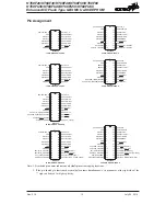
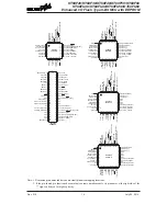
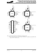
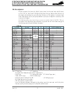
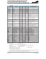
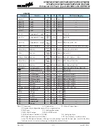
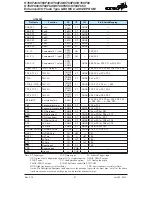
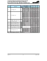
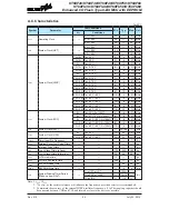
Pin Description
With the exception of the power pins, all pins on these devices can be referenced by their Port name,
e.g. PA.0, PA.1 etc, which refer to the digital I/O function of the pins. However these Port pins are
also shared with other function such as the Serial Port pins etc. The function of each pin is listed
in the following table, however the details behind how each pin is configured is contained in other
sections of the datasheet.
The following tables only include the pins which are directly related to the MCU. The pin
descriptions of the additional peripheral functions are located at the end of the datasheet along with
the relevant peripheral function functional description.
HT68F20
Pin Name
Function
OP
I/T
O/T
Pin-Shared Mapping
PA0~PA7
Port A
PAWU
PAPU
ST
CMOS
—
PB0~PB5
Port B
PBPU
ST
CMOS
—
PC0~PC3
Port C
PCPU
ST
CMOS
—
C0-� C1-
Comparator 0� 1 inp�t
CP0C
CP1C
AN
—
PA3� PC3
C0+� C1+
Comparator 0� 1 inp�t
AN
—
PA2� PC2
C0X� C1X
Comparator 0� 1 o�tp�t
—
CMOS
PA0� PA5
TCK0� TCK1
TM0� TM1 inp�t
—
ST
—
PA2� PA�
TP0_0
TM0 I/O
TMPC0
ST
CMOS
PA0
TP1_0� TP1_1
TM1 I/O
TMPC0
ST
CMOS
PA1� PC0
INT0� INT1
Ext. Interr�pt 0� 1
—
ST
—
PA3� PA�
PINT
Periphera� Interr�pt
—
ST
—
PC3
PCK
Periphera� C�ock o�tp�t
—
—
CMOS
PC2
SDI
SPI Data inp�t
—
ST
—
PA6
SDO
SPI Data o�tp�t
—
—
CMOS
PA5
SCS
SPI S�ave Se�ect
—
ST
CMOS
PB5
SCK
SPI Seria� C�ock
—
ST
CMOS
PA7
SCL
I
2
C C�ock
—
ST
NMOS
PA7
SDA
I
2
C Data
—
ST
NMOS
PA6
SCOM0~SCOM3
SCOM0~SCOM3
SCOMC
—
SCOM
PC0� PC1� PC2� PC3
OSC1
HXT/ERC pin
CO
HXT
—
PB1
OSC2
HXT pin
CO
—
HXT
PB2
XT1
LXT pin
CO
LXT
—
PB3
XT2
LXT pin
CO
—
LXT
PB�
RES
Reset inp�t
CO
ST
—
PB0
VDD
Power s�pp��
—
PWR
—
—
VSS
Gro�nd
—
PWR
—
—
Note: I/T: Input type;
O/T: Output type
OP: Optional by configuration option (CO) or register option
PWR: Power;
CO: Configuration option; ST: Schmitt Trigger input
CMOS: CMOS output;
NMOS: NMOS output
SCOM: Software controlled LCD COM;
AN: Analog input pin
HXT: High frequency crystal oscillator
LXT: Low frequency crystal oscillator
As the Pin Description Summary table applies to the package type with the most pins, not all of the above
listed pins may be present on package types with smaller numbers of pins.