Rev. 2.10
236
���� 02� 201�
Rev. 2.10
237
���� 02� 201�
HT68F20/HT68F30/HT68F40/HT68F50/HT68F60
HT68FU30/HT68FU40/HT68FU50/HT68FU60
Enhanced I/O Flash Type 8-Bit MCU with EEPROM
HT68F20/HT68F30/HT68F40/HT68F50/HT68F60
HT68FU30/HT68FU40/HT68FU50/HT68FU60
Enhanced I/O Flash Type 8-Bit MCU with EEPROM
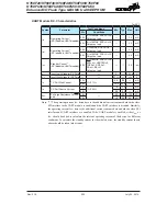
• Data, parity and stop bit selection
The format of the data to be transferred is composed of various factors such as data bit length,
parity on/off, parity type, address bits and the number of stop bits. These factors are determined
by the setup of various bits within the UCR1 register. The BNO bit controls the number of data
bits which can be set to either 8 or 9. The PRT bit controls the choice if odd or even parity. The
PREN bit controls the parity on/off function. The STOPS bit decides whether one or two stop
bits are to be used. The following table shows various formats for data transmission. The address
detect mode control bit identifies the frame as an address character. The number of stop bits,
which can be either one or two, is independent of the data length.
Start Bit
Data Bits
Address Bits
Parity Bits
Stop Bit
Example of 8-bit Data Formats
1
8
0
0
1
1
7
0
1
1
1
7
1
0
1
Example of 9-bit Data Formats
1
9
0
0
1
1
8
0
1
1
1
8
1
0
1
Transmitter Receiver Data Format
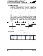
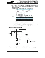
The following diagram shows the transmit and receive waveforms for both 8-bit and 9-bit data
formats.
• UART transmitter
Data word lengths of either 8 or 9 bits can be selected by programming the BNO bit in the UCR1
register. When BNO bit is set, the word length will be set to 9 bits. In this case the 9th bit, which
is the MSB, needs to be stored in the TX8 bit in the UCR1 register. At the transmitter core lies
the Transmitter Shift Register, more commonly known as the TSR, whose data is obtained from
the transmit data register, which is known as the TXR register. The data to be transmitted is
loaded into this TXR register by the application program. The TSR register is not written to with
new data until the stop bit from the previous transmission has been sent out. As soon as this stop
bit has been transmitted, the TSR can then be loaded with new data from the TXR register, if it
is available. It should be noted that the TSR register, unlike many other registers, is not directly
mapped into the Data Memory area and as such is not available to the application program for
direct read/write operations. An actual transmission of data will normally be enabled when the
TXEN bit is set, but the data will not be transmitted until the TXR register has been loaded with
data and the baud rate generator has defined a shift clock source. However, the transmission can
also be initiated by first loading data into the TXR register, after which the TXEN bit can be set.
When a transmission of data begins, the TSR is normally empty, in which case a transfer to the
TXR register will result in an immediate transfer to the TSR. If during a transmission the TXEN
bit is cleared, the transmission will immediately cease and the transmitter will be reset. The TX
output pin will then return to the high impedance state.

