Rev. 2.10
15�
���� 02� 201�
Rev. 2.10
155
���� 02� 201�
HT68F20/HT68F30/HT68F40/HT68F50/HT68F60
HT68FU30/HT68FU40/HT68FU50/HT68FU60
Enhanced I/O Flash Type 8-Bit MCU with EEPROM
HT68F20/HT68F30/HT68F40/HT68F50/HT68F60
HT68FU30/HT68FU40/HT68FU50/HT68FU60
Enhanced I/O Flash Type 8-Bit MCU with EEPROM
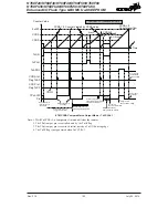
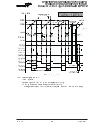
Timer/Counter Mode
To select this mode, bits TnAM1, TnAM0 and TnBM1, TnBM0 in the TMnC1 and TMnC2 register
should all be set high. The Timer/Counter Mode operates in an identical way to the Compare
Match Output Mode generating the same interrupt flags. The exception is that in the Timer/Counter
Mode the TM output pin is not used. Therefore the above description and Timing Diagrams for the
Compare Match Output Mode can be used to understand its function. As the TM output pin is not
used in this mode, the pin can be used as a normal I/O pin or other pin-shared function.
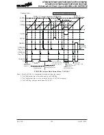
PWM Output Mode
To select this mode, the required bit pairs, TnAM1, TnAM0 and TnBM1, TnBM0 should be set
to 10 respectively and also the TnAIO1, TnAIO0 and TnBIO1, TnBIO0 bits should be set to 10
respectively. The PWM function within the TM is useful for applications which require functions
such as motor control, heating control, illumination control etc. By providing a signal of fixed
frequency but of varying duty cycle on the TM output pin, a square wave AC waveform can be
generated with varying equivalent DC RMS values.
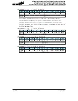
As both the period and duty cycle of the PWM waveform can be controlled, the choice of generated
waveform is extremely flexible. In the PWM mode, the TnCCLR bit is used to determine in which
way the PWM period is controlled. With the TnCCLR bit set high, the PWM period can be finely
controlled using the CCRA registers. In this case the CCRB registers are used to set the PWM duty
value (for TPnB output pins). The CCRP bits are not used and TPnA output pin is not used. The
PWM output can only be generated on the TPnB output pins. With the TnCCLR bit cleared to zero,
the PWM period is set using one of the eight values of the three CCRP bits, in multiples of 128.
Now both CCRA and CCRB registers can be used to setup different duty cycle values to provide
dual PWM outputs on their relative TPnA and TPnB pins.
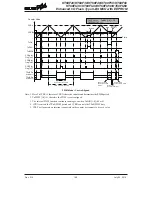
The TnPWM1 and TnPWM0 bits determine the PWM alignment type, which can be either edge
or centre type. In edge alignment, the leading edge of the PWM signals will all be generated
concurrently when the counter is reset to zero. With all power currents switching on at the same
time, this may give rise to problems in higher power applications. In centre alignment the centre
of the PWM active signals will occur sequentially, thus reducing the level of simultaneous power
switching currents.
Interrupt flags, one for each of the CCRA, CCRB and CCRP, will be generated when a compare
match occurs from either the Comparator A, Comparator B or Comparator P. The TnAOC and
TnBOC bits in the TMnC1 and TMnC2 register are used to select the required polarity of the PWM
waveform while the two TnAIO1, TnAIO0 and TnBIO1, TnBIO0 bits pairs are used to enable the
PWM output or to force the TM output pin to a fixed high or low level. The TnAPOL and TnBPOL
bit are used to reverse the polarity of the PWM output waveform.


