


Register B1 controls the dead time, it is compared with the internal counter, for a leading edge
dead time, the duty cycle of the signal is
2
(
𝑀𝐴𝑋𝐶𝑁𝑇−𝐴1
)
−𝐵1
2
(
𝑀𝐴𝑋𝐶𝑁𝑇−1
)
, where MAXCNT is the maximum value
of the time base. For a trailing edge dead time, the duty cycle of the signal is
2
(
𝑀𝐴𝑋𝐶𝑁𝑇−𝐴1
)
+𝐵1
2
(
𝑀𝐴𝑋𝐶𝑁𝑇−1
)
.
Registers A and B are buffered, they are only updated when a time base cycle ends.
A and B should be selected in a way that would not induce a roll over in the internal counter, as
this would cause unpredictable behaviour.
The configurable MODE[5] bit is as before, related to the flag generation. If it is cleared, a flag
would be generated at the trailing edge of the PWM, if it is set, a flag will be generated on both
edges.
The MODE[6] bit is for selecting between leading edge (‘1’) or trailing edge (‘0’) dead time
insertion.
1.12.
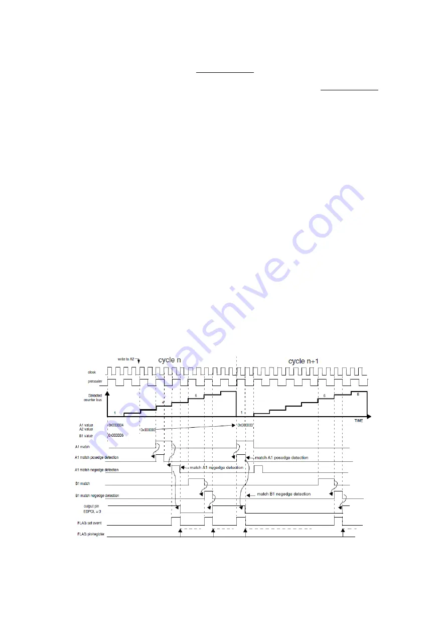
OPWMB: Output Pulse Width Modulation Buffered
The Output Pulse Width Modulation Buffered mode (MODE[0:6]=11000b0) is used for
generating PWM with variable leading and trailing edge placement. BSL should be used to select
a MCB up counting time base.
Register A1 controls the leading edge, when a match occurs between A1 and the time base, the
leading edge is generated, depending on EDPOL. Register B1 controls the trailing edge, on a
match between B1 and the time base, the trailing edge occurs.
Registers A and B are double buffered, updated on new time base cycles. A flag is generated on
B1 matches if MODE[5] is cleared, or on both matches if it is set.
Figure 61 : OPWMB mode (R.M. Rev8 – Fig. 24-44)
Summary of Contents for MPC5604B
Page 1: ...LAAS CNRS Quick Start to MPC5604B Embedded Development Sahin Serdar 21 06 2013...
Page 31: ...Figure 33 INTC SW HW mode comparison Freescale Tutorial...
Page 87: ......
Page 132: ......
Page 133: ...127 Appendix 2 Pad Configurations...
Page 134: ......
Page 135: ......
Page 136: ......
Page 137: ......
Page 138: ......
Page 139: ......
Page 140: ......
Page 141: ...Appendix 3 Peripheral input pin selection...
Page 142: ......
Page 143: ...137 Appendix 4 Interrupt Vector Table...
Page 144: ......
Page 145: ......
Page 146: ......
Page 147: ......
Page 148: ...Appendix 5 I C Baud Rate Prescaler Values...
Page 149: ......
Page 150: ......


