52
EPSON
S1C63656 TECHNICAL MANUAL
CHAPTER 4: PERIPHERAL CIRCUITS AND OPERATION (LCD Driver)
4.7.4 Display memory
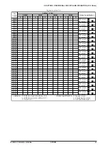
The display memory is allocated to F000H–F02FH in the data memory area and each data bit can be
allocated to an segment terminal (SEG0–SEG37) by mask option.
When a bit in the display memory is set to "1", the corresponding LCD segment goes on, and when it is
set to "0", the segment goes off.
At initial reset, the data memory content becomes undefined hence, there is need to initialize using the
software.
The display memory has read/write capability, and the addresses that have not been used for LCD
display can be used as general purpose registers.
4.7.5 Segment option
Segment allocation
The LCD driver has a segment decoder built-in, and the data bit (D0–D3) of the optional address in
the display memory area (F000H–F02FH) can be allocated to the optional segment. This makes design
easy by increasing the degree of freedom with which the liquid crystal panel can be designed.
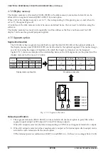
Figure 4.7.5.1 shows an example of the relationship between the LCD segments (on the panel) and the
display memory for the case of 1/4 duty.
a
f
g
e
d
p
c
SEG10
SEG11
Common
0
Common
1
Common
2
F020H
F021H
Address
d
p
D3
c
g
D2
b
f
D1
a
e
D0
Data
Display memory allocation
SEG10
SEG11
2 1 , D 1
( f )
2 0 , D 0
( a )
2 1 , D 0
( e )
2 1 , D 2
( g )
2 0 , D 2
( c )
2 0 , D 1
( b )
Pin address allocation
Common 0
Common 1
Common 2
2 0 , D 3
( d )
2 1 , D 3
( p )
Common 3
Common
3
b
Fig. 4.7.5.1 Segment allocation
Output specification
1. The segment terminals (SEG0–SEG37) can be selected with the mask option in pairs
∗
for either
segment signal output or DC output (V
DD
and V
SS
binary output).
When DC output is selected, the data corresponding to COM0 of each segment terminal is output.
2. When DC output is selected, either complementary output or N-channel open drain output can be
selected for each terminal with the mask option.
∗
The terminal pairs are combination of SEG2
×
n and SEG2
×
n + 1 (where n is an integer from 0 to 18).

