106
EPSON
S1C63656 TECHNICAL MANUAL
CHAPTER 4: PERIPHERAL CIRCUITS AND OPERATION (Integer Multiplier)
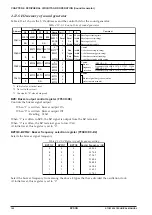
4.13.5 I/O memory of integer multiplier
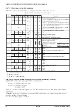
Table 4.13.5.1 shows the I/O addresses and the control bits for the integer multiplier.
Table 4.13.5.1 Control bits of integer multiplier
Address
Comment
D3
D2
Register
D1
D0
Name
Init
∗
1
1
0
DRL3
DRL2
DRL1
DRL0
–
∗
2
–
∗
2
–
∗
2
–
∗
2
Low-order 8-bit destination register
(low-order 4 bits)
LSB
R/W
FF82H
DRL3
DRL2
DRL1
DRL0
DRL7
DRL6
DRL5
DRL4
–
∗
2
–
∗
2
–
∗
2
–
∗
2
MSB
Low-order 8-bit destination register
(high-order 4 bits)
R/W
FF83H
DRL7
DRL6
DRL5
DRL4
SR3
SR2
SR1
SR0
–
∗
2
–
∗
2
–
∗
2
–
∗
2
Source register (low-order 4 bits)
LSB
R/W
FF80H
SR3
SR2
SR1
SR0
SR7
SR6
SR5
SR4
–
∗
2
–
∗
2
–
∗
2
–
∗
2
MSB
Source register (high-order 4 bits)
R/W
FF81H
SR7
SR6
SR5
SR4
FF86H
NF
VF
ZF
CALMD
R
R/W
NF
VF
ZF
CALMD
0
0
0
0
Negative
Overflow
Zero
Run
Div.
Positive
No
No
Stop
Mult.
Negative flag
Overflow flag
Zero flag
Operation status (reading)
Calculation mode selection (writing)
DRH3
DRH2
DRH1
DRH0
–
∗
2
–
∗
2
–
∗
2
–
∗
2
High-order 8-bit destination register
(low-order 4 bits)
LSB
R/W
FF84H
DRH3
DRH2
DRH1
DRH0
DRH7
DRH6
DRH5
DRH4
–
∗
2
–
∗
2
–
∗
2
–
∗
2
MSB
High-order 8-bit destination register
(high-order 4 bits)
R/W
FF85H
DRH7
DRH6
DRH5
DRH4
*1 Initial value at initial reset
*2 Not set in the circuit
*3 Constantly "0" when being read
SR0–SR7: Source register (FF80H, FF81H)
Used to set multipliers and divisors.
Set the low-order 4 bits of data to SR0–SR3 and the high-order 4 bits to SR4–SR7.
This register maintains the latest set value until the next writing, so it is not necessary to set data for each
operation if the same multiplier and divisor is used in a series of operations.
At initial reset, this register is undefined.
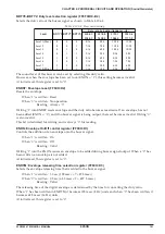
DRL0–DRL7: Destination register low-order 8 bits (FF82H, FF83H)
Used to set multiplicands and low-order 8 bits of dividends.
Set the low-order 4 bits of data to DRL0–DRL3 and the high-order 4 bits to DRL4–DRL7.
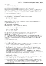
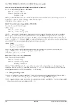
Data written to this register is loaded to the arithmetic circuit when an operation starts (by writing to
FF86H•D0), and then a multiplication or a division is performed in 10 CPU clock cycles (5 bus cycles).
After the operation has finished, the low-order 8 bits of the product or the quotient are loaded to this
register.
However, if an overflow occurs in a division process, the quotient is not loaded and the low-order 8 bits
of the dividend remains.
At initial reset, this register is undefined.

