S1C63656 TECHNICAL MANUAL
EPSON
31
CHAPTER 4: PERIPHERAL CIRCUITS AND OPERATION (Oscillation Circuit)
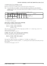
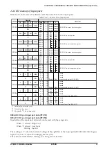
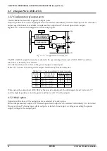
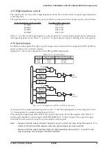
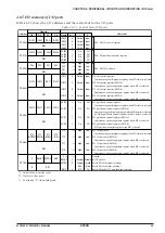
4.3.6 I/O memory of oscillation circuit
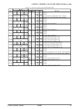
Table 4.3.6.1 shows the I/O address and the control bits for the oscillation circuit.
Note: The control bits for the oscillation circuit described below are effective only when the OSC3
oscillation circuit is used. If the system uses the OSC1 oscillation circuit only, do not change the
default settings.
Table 4.3.6.1 Control bits of oscillation circuit
Address
Comment
D3
D2
Register
D1
D0
Name
Init
∗
1
1
0
FF01H
CLKCHG OSCC
0
0
R/W
R
CLKCHG
OSCC
0
∗
3
0
∗
3
0
0
–
∗
2
–
∗
2
OSC3
On
OSC1
Off
CPU clock switch
OSC3 oscillation On/Off
Unused
Unused
*1 Initial value at initial reset
*2 Not set in the circuit
*3 Constantly "0" when being read
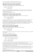
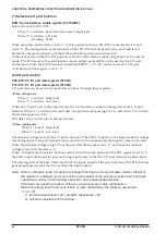
OSCC: OSC3 oscillation control register (FF01H•D2)
Turns the OSC3 oscillation circuit on and off.
When "1" is written: OSC3 oscillation On
When "0" is written: OSC3 oscillation Off
Reading: Valid
When it is necessary to operate the CPU at high speed, set OSCC to "1". At other times, set it to "0" to
reduce current consumption.
At initial reset, this register is set to "0".
CLKCHG: CPU system clock switching register (FF01H•D3)
The CPU's operation clock is selected with this register.
When "1" is written: OSC3 clock is selected
When "0" is written: OSC1 clock is selected
Reading: Valid
When the CPU clock is to be OSC3, set CLKCHG to "1"; for OSC1, set CLKCHG to "0".
After turning the OSC3 oscillation on (OSCC = "1"), switching of the clock should be done after waiting 5
msec or more.
At initial reset, this register is set to "0".


