S1C63656 TECHNICAL MANUAL
EPSON
89
CHAPTER 4: PERIPHERAL CIRCUITS AND OPERATION (Serial Interface)
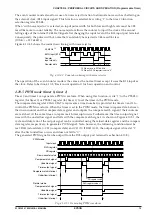
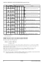
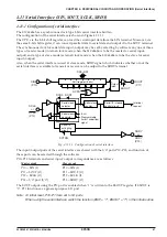
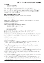
A sample basic serial input/output portion connection is shown in Figure 4.11.3.1.
S1C63656
SCLK
SOUT
SIN
Input terminal
External
serial device
CLK
SOUT
SIN
READY
S1C63656
SCLK
SOUT
SIN
SRDY
External
serial device
CLK
SOUT
SIN
Input terminal
(a) Master mode
(b) Slave mode
Fig. 4.11.3.1 Sample basic connection of serial input/output section
4.11.4 Data input/output and interrupt function
The serial interface of S1C63656 can input/output data via the internal 8-bit shift register. The shift
register operates by synchronizing with either the synchronous clock output from the SCLK (P12) termi-
nal (master mode), or the synchronous clock input to the SCLK (P12) terminal (slave mode).
The serial interface generates an interrupt on completion of the 8-bit serial data input/output. Detection
of serial data input/output is done by counting of the synchronous clock SCLK; the clock completes
input/output operation when 8 counts (equivalent to 8 cycles) have been made and then generates an
interrupt.
The serial data input/output procedure is explained below:
Serial data output procedure and interrupt
The S1C63656 serial interface is capable of outputting parallel data as serial data, in units of 8 bits.
By setting the parallel data to the data registers SD0–SD3 (FF72H) and SD4–SD7 (FF73H) and writing
"1" to SCTRG bit (FF70H•D1), it synchronizes with the synchronous clock and the serial data is output
to the SOUT (P11) terminal. The synchronous clock used here is as follows: in the master mode,
internal clock which is output to the SCLK (P12) terminal while in the slave mode, external clock
which is input from the SCLK (P12) terminal.
Shift timing of serial data is as follows:
• When positive polarity is selected for the synchronous clock (mask option):
The serial data output to the SOUT (P11) terminal changes at the rising edge of the clock input or
output from/to the SCLK (P12) terminal. The data in the shift register is shifted at the rising edge of
the SCLK signal when the SCPS register is "1" and is shifted at the falling edge of the SCLK signal
when the SCPS register is "0".
• When negative polarity is selected for the synchronous clock (mask option):
The serial data output to the SOUT (P11) terminal changes at the falling edge of the clock input or
_________
output from/to the SCLK (P12) terminal. The data in the shift register is shifted at the falling edge of
_________
the SCLK signal when the SCPS register (FF71H•D2) is "1" and is shifted at the rising edge of the
_________
SCLK signal when the SCPS register is "0".
When the output of the 8-bit data from SD0 to SD7 is completed, the interrupt factor flag ISIF
(FFF2H•D0) is set to "1" and an interrupt occurs. Moreover, the interrupt can be masked by the
interrupt mask register EISIF (FFE2H•D0). However, regardless of the interrupt mask register setting,
the interrupt factor flag is set to "1" after output of the 8-bit data.

