


Power
Mains
Leakage
Capacitances to
Earth Ground
C
leak,GND
C
load
PLT-22 and Power Supply
Node
Logic
Ground
C
decouple
C
leak,SIGNAL
V
gate
VDD5
GND
"CHASSIS"
GND
C
leak,CHASSIS
L
N
C
ou
p
lin
g
C
ir
cu
it
VDD5
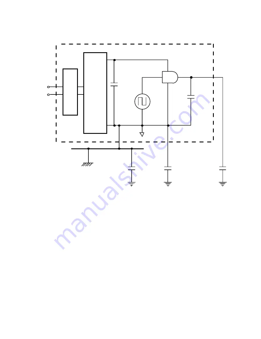
Figure 6.1
Parasitic Leakage Capacitances to Earth Ground
From this discussion, it is apparent that minimizing C
leak,SIGNAL
is very important.
By using 0.1µF or 0.01µF decoupling capacitors at each digital IC power pin, V
DD5
and logic ground noise can be reduced. Logic ground can then be used as a ground
shield for other noisy digital signals and clock lines.
For example, in most PLT-22 transceiver-based nodes that use the Neuron 3120
Chip, the fastest digital signal on the PCB is the CKOUT line from the PLT-22
transceiver to the Neuron Chip. If a two-layer PCB is being used, CKOUT can be
routed to the Neuron Chip with ground guard traces straddling the clock trace on the
component side of the board, and a wide ground trace (or ground plane) covering the
underside of the clock trace on the solder side of the PCB. If a four-layer PCB is
used, the clock trace can be moved to an inner layer and guarded on all four sides.
The CKOUT line from the PLT-22 transceiver to the Neuron Chip should be as short
as practical, and in all cases
≤
50mm (2").
Since the Neuron 3150 Chip has an external memory interface bus, there are many
more traces in a node using a Neuron 3150 Chip that need to be guarded by logic
ground. In addition, the V
DD5
noise generated by the memory interface and external
ROM/RAM components requires more V
DD5
decoupling, and may require a four-
layer PCB to maintain RF-quiet V
DD5
and logic ground lines.
L
ON
W
ORKS
PLT-22 Transceiver User’s Guide
6-3
Summary of Contents for LONWORKS PLT-22
Page 6: ...iv Echelon...
Page 14: ...1 8 Introduction...
Page 67: ...LONWORKS PLT 22 Transceiver s User Guide 5 7 Figure 5 3 Capacitor Input Power Supply Schematic...
Page 92: ...6 10 Design and Test for Electromagnetic Compatibility...
Page 110: ...7 18 Communication Performance Verification...
Page 114: ...8 4 References...
Page 118: ...A 4 Appendix A...


