PCM-3362 User Manual
44
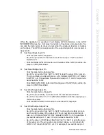
and 1 high, 3 to low, the pin number should be ‘0x0B/, and then you should
key in the value ‘0x0A’ to write.
–
Click the WRITE GPIO DATA button to write the GPIO output pins.
I
2
C
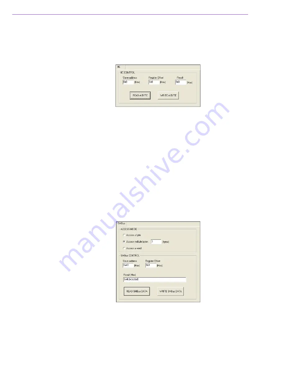
When the application is executed, you can read or write a byte of data through I2C
devices. All data must be read or written in hexadecimal system.
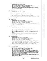
Read a byte
–
Key in the slave device address in Slave address field.
–
Key in the register offset in Register Offset field.
–
Click the READ A BYTE button and then a byte of data from the device will
be shown on the Result field.
Write a byte
–
Key in the slave device address in Slave address field.
–
Key in the register offset in Register Offset field.
–
Key in the desirous of data in Result field to write to the device.
–
Click the WRITE A BYTE button and then the data will be written to the
device through I
2
C.
SMBus
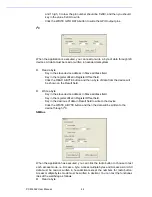
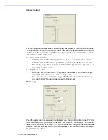
When the application has executed, you can click the radio button to choose to test
each access mode, i.e. Access a byte, Access multiple bytes and Access a word. All
data must be read or written in hexadecimal except the numbers for radio button:
Access multiple bytes mode must be written in decimal. You can test the functional-
ities of the watchdog as follows:
Read a byte
Summary of Contents for PCM-3362
Page 1: ...Data Modul AG www data modul com Specification PCM 3362 ...
Page 13: ...PCM 3362 User Manual 6 ...
Page 14: ...Chapter 2 2 Hardware Installation ...
Page 23: ...PCM 3362 User Manual 16 ...
Page 24: ...Chapter 3 3 AMI BIOS Setup ...
Page 44: ...Chapter 4 4 Software Introduction Installation ...
Page 55: ...PCM 3362 User Manual 48 ...
Page 56: ...Chapter 5 5 Chipset Software Installation Utility ...
Page 58: ...Chapter 6 6 Integrated Graphic Device Setup ...
Page 60: ...Chapter 7 7 LAN Configuration ...
Page 75: ...PCM 3362 User Manual 68 ...
Page 76: ...Appendix C C Mechanical Drawings ...
Page 81: ...PCM 3362 User Manual 74 ...
Page 82: ...Appendix D D Watchdog Timer and GPIO sample code ...

