background image

33

PCM-3362 User Manual

Chapter 3

A

MI BIOS

Setup

3.7

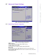
Advanced Chipset Settings 

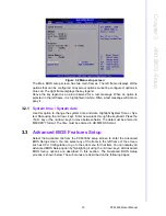
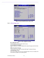
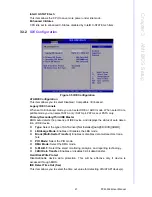
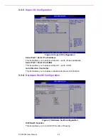
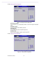
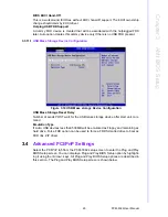
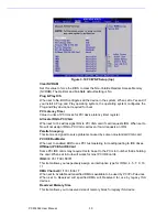
Figure 3.23 Advanced Chipset Settings 

3.7.1

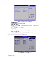
North Bridge Chipset Configuration

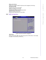
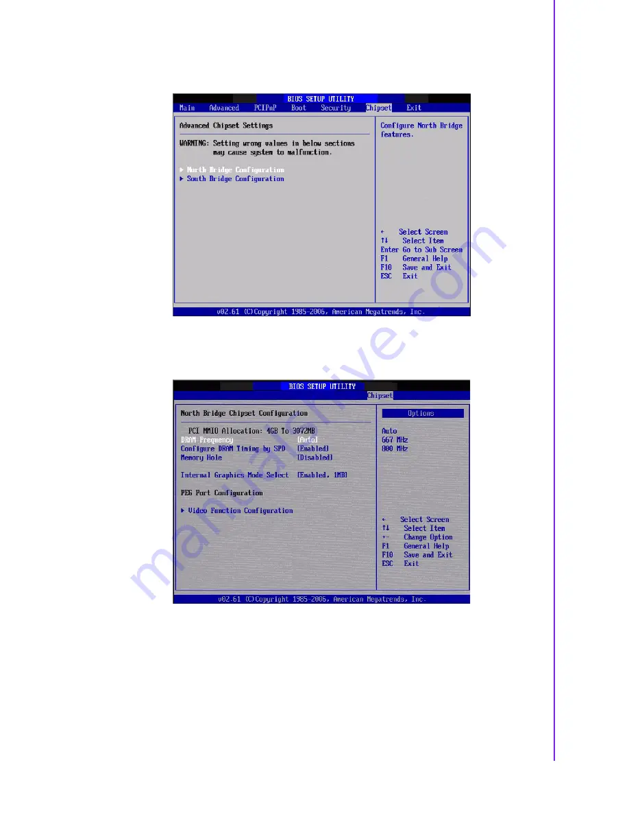
Figure 3.24 North Bridge Configuration

DRAM Frequency

This item allows you to manually changed DRAM frequency.

Configure DRAM Timing by SPD

This item allows you to enables or disables detect by DRAM SPD.

Memory Hole

This item allows you to free 15MB-16MB of memory size for some ISA devices.

Internal Graphics Mode Select:

 Select the amount of system memory used by the

Internal graphics device. 

Summary of Contents for PCM-3362

Page 1: ...Data Modul AG www data modul com Specification PCM 3362 ...

Page 2: ...software etc A complete description of the problem The exact wording of any error messages Declaration of Conformity This device complies with the requirements in part 15 of the FCC rules Operation is subject to the following two conditions 1 This device may not cause harmful interference and 1 x PCM 3362 SBC 1 x SATA data cable p n 1700071000 1 x SATA power cable p n 1703150102 1 x Keyboard Mouse...

Page 3: ...s uses and can radiate radio frequency energy and if not installed and used in accordance with the instruc tion manual may cause harmful interference to radio communications Opera thin of this equipment in a residential area is likely to cause harmful interference in which case the user will be required to correct the interference at his own expense Caution There is a danger of a new battery explo...

Page 4: ... Panel Power Select JP2 11 Table 2 4 LVDS Panel Power Select JP2 11 2 4 3 COM3 RS422 RS485 Select JP3 12 Table 2 5 COM3 RS422 RS485 Select JP3 12 2 4 4 PCI I O Voltage Select JP4 12 Table 2 6 PCI I O Voltage Select JP4 12 2 5 Installing SODIMMs 12 2 6 Flash 12 2 7 High Definition Audio Interface CN1 13 2 8 VGA LCD interface connections 13 2 8 1 CRT display connector CN8 13 2 8 2 LVDS connector CN6...

Page 5: ... 3 3 8 Event Log Configuration 27 Figure 3 14South Bridge ACPI Configuration 27 3 3 9 MPS Configuration 27 Figure 3 15South Bridge ACPI Configuration 27 3 3 10 Smbios Configuration 28 Figure 3 16South Bridge ACPI Configuration 28 3 3 11 USB Configuration 28 Figure 3 17South Bridge ACPI Configuration 28 Figure 3 18USB Mass storage Device Configuration 29 3 4 Advanced PCI PnP Settings 29 Figure 3 19...

Page 6: ...n 54 7 2 Installation 54 7 3 Windows XP Vista Win7 Driver Setup 54 Appendix A Pin Assignments 55 A 1 Jumper and Connector Tables 56 Appendix B System Assignments 65 B 1 System I O Ports 66 Table B 1 System I O ports 66 B 2 1st MB Memory Map 66 Table B 2 1st MB memory map 66 B 3 DMA channel assignments 66 Table B 3 DMA channel assignments 66 B 4 Interrupt assignments 67 Table B 4 Interrupt assignme...

Page 7: ...PCM 3362 User Manual viii Appendix D Watchdog Timer and GPIO sample code 75 D 1 Watchdog Timer sample code 76 D 2 GPIO sample code 77 ...

Page 8: ...Chapter 1 1 General Information This chapter gives background information on the PCM 3362 Sections include Introduction Features Specifications Board layout and dimensions ...

Page 9: ...I Os and includes a single 10 100 1000 Mbps Ethernet four USB Universal Serial Bus 2 0 one SATA2 interface 8 bit general purpose Input Output two RS 232 serial ports and one RS 422 485 serial port for easy system expansibility PC 104 plus self stack ing rugged mechanical architecture and extended temperature operation makes it ideal for outdoor applications in the military and transportation field...

Page 10: ...ed graphic core of Embedded Gen3 5 technology VRAM 224 MB shared system memory Output Interfaces VGA Supports up to SXGA 1400 x 1060 60Hz LVDS Singe channel 18 bit LVDS up to WXGA 1366 x 768 Dual Display CRT LVDS support extended mode and clone mode 1 3 3 Ethernet Interface Supports Single 10 100 1000 Mbps Ethernet networking Controller Intel 82567V 1 3 4 OS support This board supports Win7 Win XP...

Page 11: ...stem under maxi mum load CPU Top speed RAM Graphic Full loading Idle mode Measure the current value when system in windows mode and without running any program Operating temperature 0 60 C 32 140 F operation humidity 40 C 85 RH Non Condensing Weight 0 85 kg reference weight of total package 1 4 Board layout dimensions Figure 1 1 Board layout Dimensions Component Side ...

Page 12: ...5 PCM 3362 User Manual Chapter 1 General Information Figure 1 2 Board layout Dimensions Solder Side ...

Page 13: ...PCM 3362 User Manual 6 ...

Page 14: ...Chapter 2 2 Hardware Installation ...

Page 15: ...rives The table below lists the function of each of the board s connectors Table 2 1 Jumpers JP1 CLEAR CMOS JP2 LVDS Panel Power Select JP3 COM3 RS422 RS485 Select JP4 PCI I O Voltage Select Table 2 2 Connectors Label Function CN1 HD Audio Connector CN4 SO DIMM Connector CN6 LVDS Connected CN7 Panel Inverter Connector CN8 VGA Connector CN9 USB Port0 1 Connector CN10 USB Port2 3 Connector CN12 Fron...

Page 16: ...9 PCM 3362 User Manual Chapter 2 Hardware Installation 2 3 Locating Connectors block diagram Figure 2 1 Connectors component side Figure 2 2 Connectors solder side ...

Page 17: ... to close an electric circuit It consists of two metal pins and a small metal clip often protected by a plastic cover that slides over the pins to connect them To close a jumper you connect the pins with the clip To open a jumper you remove the clip Sometimes a jumper will have three pins labeled 1 2 and 3 In this case you would connect either pins 1 and 2 or 2 and 3 FORVHG FORVHG RSHQ ...

Page 18: ...PCM 3362 single board computer contains a jumper that can erase CMOS data and reset the system BIOS information Normally this jumper should be set with pins 1 2 closed If you want to reset the CMOS data set CMOS1 to 2 3 closed for just a few seconds and then move the jumper back to 1 2 closed This procedure will reset the CMOS to its default setting 2 4 2 LVDS Panel Power Select JP2 Open Closed Cl...

Page 19: ...tline Dual In line Memory Modules 1 Ensure that all power supplies to the system are switched off 2 Tilt the SODIMM card just above the board and slide it into the housing card slot 3 Push the module into the socket until the module gently snaps in There should only be a slight insertion force to engage the module into the contacts Make sure that the module and the housing are aligned and locked i...

Page 20: ...ive scan analog monitor with pixel resolution up to SXGA 1400 x 1060 60Hz Pin assignments for CRT display connector CN8 are detailed in Appendix A 2 8 2 LVDS connector CN6 The PCM 3362 uses the Intel Atom N450 that supports single channel 18 bit LVDS panel up to WXGA 1366 x 768 UXGA panel resolution 2 8 3 Panel Inverter Power CN7 The LCD inverter is connected to CN7 via a 5 pin connector to provid...

Page 21: ...gnments for the COM port connector in Appendix 2 13 1 Serial Port RS 422 485 CN17 COM3 CN17 can be configured to operate in RS 422 or RS 485 mode by JP3 2 14 Giga LAN Connector CN18 PCM 3362 uses the Intel 82567V Gigabit LAN chips are linked to dedicated PCIe x1 lanes PCM 3362 provide high throughputs for heavy loading networking environ ment LAN connections are made via two internal 10 pin box he...

Page 22: ...2C Bus connector CN25 PCM 3362 provides I2C Bus connector for customer connection to I2C protocol embedded device Advantech also provide I2C API allowing a developer to interface with an embedded system environment and transfer serial messages using the I2C protocols allowing multiple simultaneous device control 2 20 12 V 5 V power connector CN26 The PCM 3362 is equipped with a Negative Power Inpu...

Page 23: ...PCM 3362 User Manual 16 ...

Page 24: ...Chapter 3 3 AMI BIOS Setup ...

Page 25: ...etup Turn on the computer and check for the patch code If there is a number assigned to the patch code it means that the BIOS supports your CPU If there is no number assigned to the patch code please contact an Advantech application engineer to obtain an up to date patch code file This will ensure that your CPU s system status is valid After ensuring that you have a number assigned to the patch co...

Page 26: ...Highlight System Time or Sys tem Date using the Arrow keys Enter new values through the keyboard Press the Tab key or the Arrow keys to move between fields The date must be entered in MM DD YY format The time must be entered in HH MM SS format 3 3 Advanced BIOS Features Setup Select the Advanced tab from the PCM 3362 setup screen to enter the Advanced BIOS Setup screen You can select any of the it...

Page 27: ...UID maximum value Execute Disable Bit Capability This item allows you to enable or disable the No Execution page protection technol ogy Hyper Threading Technology This item allows you to enable or disable Intel Hyper Threading technology Intel SpeedStepTM tech When set to disabled the CPU runs at its default speed when set to enabled the CPU speed is controlled by the operating system ...

Page 28: ...hird IDE Master BIOS auto detects the presence of IDE device and displays the status of auto detec tion of IDE device Type Select the type of SATA driver Not Installed Auto CD DVD ARMD LBA Large Mode Enables or Disables the LBA mode Block Multi Sector Transfer Enables or disables data multi sectors trans fers PIO Mode Select the PIO mode DMA Mode Select the DMA mode S M A R T Select the smart moni...

Page 29: ...ort1 port3 of base addresses Serial Port1 Port2 Port3 IRQ This item allows you to select serial port1 port3 of IRQ Auto Direction Control Sel This item allows you to enable or disable auto flow control function 3 3 4 Hardware Health Configuration Figure 3 7 Hardware health configuration H W Health Function This item allows you to control H W monitor of showing ...

Page 30: ...re Vcore 3 3Vin 5Vin 12Vin VBAT 3 3 5 ACPI Settings Figure 3 8 ACPI Settings 3 3 5 1 General ACPI Configuration Figure 3 9 General ACPI Configuration Suspend mode Select the ACPI state used for system suspend Report Video on S3 Resume This item allows you to invoke VA BIOS POST on S3 STR resume ...

Page 31: ...ou to enable RSDP pointers to 64 bit fixed system description tables ACPI APIC support Include APIC table pointer to RSDT pointer list AMI OEMB table Include OEMB table pointer to R x SDT pointer lists Headless mode Enable Disable Headless operation mode through ACPI 3 3 5 3 Chipset ACPI Configuration Figure 3 11 Chipset ACPI Configuration ...

Page 32: ...sable APIC ACPI SCI IRQ USB Device Wakeup From S3 S4 Enable Disable USB Device Wakeup from S3 S4 High Performance Event Timer Enable Disable High performance Event timer 3 3 6 AHCI Configuration Figure 3 12 Advanced ACPI Configuration AHCI Ports0 While entering setup BIOS auto detects the presence of IDE devices This displays the status of auto detection of IDE device ...

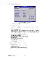
Page 33: ...ff after power failure the On setting boots up the system after failure and the Last State returns the system to the status just before power failure Video Power Down Mode Power down video in suspend or standby mode Hard Disk Power Down Mode Power down Hard Disk in suspend or standby mode Standby Time Out Go into standby in the specified time Suspend Time Out Go into Suspend in the specified time ...

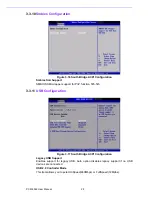
Page 34: ...ACPI Configuration View Event Log View all unread events on the event Log Mark all events as read Mark all unread events as read Clear Event Log Discard all events in the event Log 3 3 9 MPS Configuration Figure 3 15 South Bridge ACPI Configuration MPS Revision This item allows you to select MPS reversion ...

Page 35: ... SMI wrapper support for PnP function 50h 54h 3 3 11 USB Configuration Figure 3 17 South Bridge ACPI Configuration Legacy USB Support Enables support for legacy USB Auto option disables legacy support if no USB devices are connected USB 2 0 Controller Mode This item allows you to select HiSpeed 480Mbps or FullSpeed 12Mpbs ...

Page 36: ...guration USB Mass Storage Reset Delay Number of sends POST wait for the USB mass storage device after start unit com mand Emulation Type If Auto USB devices less than 530MB will be emulated as Floppy and remaining as hard drive Force FDD option can be used to force a FDD formatted drive to boot as FDD Ex ZIP drive 3 4 Advanced PCI PnP Settings Select the PCI PnP tab from the PCM 3362 setup screen ...

Page 37: ...ll not assign IRQ to PCI VGA card even if card requests an IRQ Palette Snooping This item is designed to solve problems caused by some non standard VGA card PCI IDE BusMaster When set to enabled BIOS uses PCI busmastering for reading writing to IDE drives OffBoard PCI ISA IDE Card Some PCI IDE cards may require this to be set to the PCI slot number that is holding the card When set to Auto will wo...

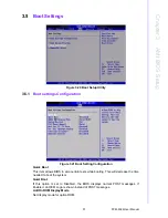
Page 38: ...Boot Setting Configuration Quick Boot This item allows BIOS to skip certain tests while booting This will decrease the time needed to boot the system Quiet Boot If this option is set to Disabled the BIOS displays normal POST messages If Enabled an OEM Logo is shown instead of POST messages AddOn ROM Display Mode Set display mode for option ROM ...

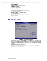
Page 39: ...ootsafe function This item allows you to enables or disables bootsafe function 3 6 Security Setup Figure 3 22 Password Configuration Select Security Setup from the PCM 3362 Setup main BIOS setup menu All Security Setup options such as password protection and virus protection are described in this section To access the sub menu for the following items select the item and press Enter Change Supervis...

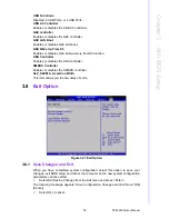
Page 40: ...th Bridge Configuration DRAM Frequency This item allows you to manually changed DRAM frequency Configure DRAM Timing by SPD This item allows you to enables or disables detect by DRAM SPD Memory Hole This item allows you to free 15MB 16MB of memory size for some ISA devices Internal Graphics Mode Select Select the amount of system memory used by the Internal graphics device ...

Page 41: ...DVMT FIXED system memory to allocate for video memory Boot Display Device Select boot display device at post stage Flat Panel Type This item allows you to select which panel resolution you wants Spread Spectrum Clock This item allows you to enables or disables spread spectrum clock 3 7 2 South Bridge Chipset Configuration Figure 3 26 South Bridge Configuration ...

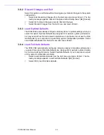
Page 42: ...s the HDA controller SMBUS Controller Enables or disables the SMBUS controller SLP_S4 Min Assertion Width This item allows you to set a delay of sorts 3 8 Exit Option Figure 3 27 Exit Option 3 8 1 Save Changes and Exit When you have completed system configuration select this option to save your changes exit BIOS setup and reboot the computer so the new system configuration parameters can take effe...

Page 43: ...ts are designed for maximum system performance but may not work best for all computer applications In particular do not use the Opti mal Defaults if your computer is experiencing system configuration problems Select Load Optimal Defaults from the Exit menu and press Enter 3 8 4 Load Fail Safe Defaults The PCM 3362 automatically configures all setup options to fail safe settings when you select thi...

Page 44: ...Chapter 4 4 Software Introduction Installation ...

Page 45: ...mmers Advantech has released a suite of API Application Programming Interface in the form of a program library The program Library is called Secured and Unified Smart Interface or SUSI for short In modern operating systems user space applications cannot access hardware directly Drivers are required to access hardware User space applications access hardware through drivers Different operating syste...

Page 46: ...2 3 The Display Control API There are two kinds of VGA control APIs backlight on off control and brightness con trol Backlight on off control allows a developer to turn on or off the backlight and to control brightness smoothly 1 Brightness Control The Brightness Control API allows a developer to interface with an embed ded device to easily control brightness 2 Backlight Control The Backlight API ...

Page 47: ...device if critical errors happen and are not solved immediately permanent damage may be caused 4 3 3 3 eSOS The eSOS is a small OS stored in BIOS ROM It will boot up in case of a main OS crash It will diagnose the hardware status and then send an e mail to a designated administrator The eSOS also provides remote connection Telnet server and FTP server allowing the administrator to rescue the syste...

Page 48: ... to add a new category e g the SUSI Library Then you can add a new file in this category and upload the SUSI dll for this category After these steps you can select the SUSI Library category you created for every project Manual Installation You can add the SUSI Library into the image by editing any bib file First you open project bib in the platform builder Add this line to the MODULES section of p...

Page 49: ...d it requires the shared library Susi dll to demonstrate the SUSI functions The source code of SusiDemo exe also has two versions i e Windows CE and Windows XP and must be compiled under Microsoft Visual C 6 0 on Windows XP or under Microsoft Embedded Visual C 4 0 on Windows CE Developers must add the header file Susi h and library Susi lib to their own projects when they want to develop something...

Page 50: ... 1 stands for GPIO 1 etc For example if you want to read pin 0 1 and 3 the pin num bers should be 0x0B Click READ GPIO DATA button and the statuses of the GPIO pins will be dis played in R W Result field Test Write Single Output Pin Click the radio button Single Pin Key in the pin numbers you want to write Pin numbers start from 0 Key in the value either 0 or 1 in R W Result field to write the out...

Page 51: ...ata from the device will be shown on the Result field Write a byte Key in the slave device address in Slave address field Key in the register offset in Register Offset field Key in the desirous of data in Result field to write to the device Click the WRITE A BYTE button and then the data will be written to the device through I2 C SMBus When the application has executed you can click the radio butt...

Page 52: ...egister offset in the Register Offset field Key in the desired data such as 0x1234 in the Result field to write to the device Click the WRITE SMBus DATA button and the data will be written to the device through the SMBus Read Multiple bytes Click the radio button Access multiple bytes Key in the slave device address in the Slave address field Key in the register offset in the Register Offset field...

Page 53: ...ay chip of your platform must be in the support list in Appendix A or this function cannot work Brightness control Move the slider in increments using either the mouse or the direction keys or click the UP button to increase the brightness Move the slider in decrements using either the mouse or the direction keys or click the DOWN button to decrease the brightness Watchdog When the application is ...

Page 54: ...EFRESH button After you click this button the Timeout Countdown field will display the value of the SET TIMEOUT field If you want to stop the watchdog timer you just click the STOP button Hardware Monitor CL When the Monitor application is executed by clicking the button hardware monitoring data values will be displayed If certain data values are not supported by the platform the correspondent dat...

Page 55: ...PCM 3362 User Manual 48 ...

Page 56: ...Chapter 5 5 Chipset Software Installation Utility ...

Page 57: ...et Software Installation CSI utility installs the Windows INF files that outline to the operating system how the chipset components will be configured This is needed for the proper functioning of the following features Core PCI PnP services Serial ATA interface support USB 1 1 2 0 support USB 2 0 driver needs to be installed separately for Win98 Identification of Intel chipset components in the De...

Page 58: ...Chapter 6 6 Integrated Graphic Device Setup ...

Page 59: ... highlight the igxp32 INF if 32 bit or igxp64 INF if 64 bit Click on the Open button 3 Click on the OK button A window listing all of the available display types should open Select the display adapter that your system contains and then click on the Next button 4 Click on the Next button The operating system will install the driver Click on the Finish button when done 5 Click on the Close button an...

Page 60: ...Chapter 7 7 LAN Configuration ...

Page 61: ...However the installation procedure varies with different operating systems Please find and use the section that provides the driver setup procedure for the oper ating system you are using 7 3 Windows XP Vista Win7 Driver Setup Insert the driver CD into your system s CD ROM drive You can see the driver folder items Navigate to the PCM 3362 03 LAN folder and click autorun program to com plete the in...

Page 62: ...Appendix A A Pin Assignments This appendix contains informa tion of a detailed or specialized nature Sections include Jumper and Connector Tables ...

Page 63: ...2 LVDS PANEL POWER Select Part Number 1653003101 Footprint JH3X1V 2M Description PIN HEADER 3 1P 180D M 2 0mm DIP SQUARE W O Pb Setting Function 1 2 5V for VLVDS_PANEL POWER Select 2 3 3 3V for VLVDS_PANEL POWER Select Default JP3 COM3 RS422 RS485 Select Part Number 1653003101 Footprint JH3X1V 2M Description PIN HEADER 3 1P 180D M 2 0mm DIP SQUARE W O Pb Setting Function 1 2 RS485 default 2 3 RS42...

Page 64: ... 2 0mm DIP 209 1 8GS Pin Pin Name Signal Type Signal Level 1 V5 PWR 5 V 2 GND 3 AZ_BITCLK CLK 4 AZ_SYNC I O 5 AZ_RST I O 6 AZ_SDIN0 IN 7 AZ_SDOUT OUT 8 V12 PWR 12 V CN4 DDR2 SO DIMM Part Number 1651000087 Footprint DDR SODIMM STD65 Description SKT DIMM 200P DDR2 H 6 5mm STD SMD WO Pb CN6 LVDS Connector Part Number 1653910261 Footprint SPH10X2 Description CONN SMD 10 2P 180D M DF13 20DP 1 25V 91 HR...

Page 65: ...X 2 0mm 5P 180D M W LOCK Pin Pin Name Signal Type Signal Level 1 V12_INVERTER PWR 12V 2 GND GND 3 LVDS0_ENABKL OUT 3 3V 4 LVDS0_VBR OUT 3 3V 5 V5_INVERTER PWR 5V CN8 VGA Connector Part Number 1655912120 Footprint WB12P S1 25mm Description Wafer Box 1 25mm 12P 90D M SMD 85204 12001 Pin Pin Name Signal Type Signal Level 1 GND GND 2 VGA_z_R OUT 5 V 3 VGA_z_G OUT 5 V 4 VGA_z_B OUT 5 V 5 GND GND 6 V5_C...

Page 66: ... PWR 5 V 2 V5_USB0 PWR 5 V 3 USB0_z_P I O 4 USB1_z_P I O 5 USB0_z_P I O 6 USB1_z_P I O 7 GND 8 GND 9 GND CN10 USB2 3 Part Number 1653003718 Footprint PH5x2P SR2 00 Description PIN HEADER 5 2P 2 00mm 90D M NO 10 SMD Pin Pin Name Signal Type Signal Level 1 V5_USB0 PWR 5 V 2 V5_USB0 PWR 5 V 3 USB2_z_P I O 4 USB3_z_P I O 5 USB2_z_P I O 6 USB3_z_P I O 7 GND 8 GND 9 GND 3 6 4 5 2 8 9 7 10 1 3 6 4 5 2 8 ...

Page 67: ...UT CN13 Buzzer Connector Part Number 1653002101 Footprint HD_2x1P_79_D Description PIN HEADER 2 1P 180D M SQUARE 2 0mm DIP W O Pb Pin Pin Name Signal Type Signal Level 1 V3 3 PWR 3 3 V 2 SB_z_SPKR OUT CN15 SATA1 connector Part Number 1654000128 Footprint SATA LD11071S02 Description Serial ATA 7P 90D M SMD 15u Reverse Pin Pin Name Signal Type Signal Level 1 GND GND 2 SATA0_TX I O Analog 3 SATA0_TX ...

Page 68: ... 5 V 6 COM0_CTS IN 5 V 7 COM0_DTR I O 5 V 8 COM0_RI IN 5 V 9 GND 10 GND 11 COM1_DCD IN 5 V 12 COM1_DSR IN 5 V 13 COM1_RXD IN 5 V 14 COM1_RTS I O 5 V 15 COM1_TXD OUT 5 V 16 COM1_CTS IN 5 V 17 COM1_DTR I O 5 V 18 COM1_RI IN 5 V 19 GND 20 GND CN17 RS422 485 Connector Part Number 1655304120 Footprint WHL4H 2M_A Description WAFER BOX 2 0mm 4P 90D M DIP W LOCK Pin Pin Name Signal Type Signal Level 1 RS4...

Page 69: ...log A9 LAN1_M0 I O Analog A10 LAN1_M0 I O Analog CN19 LAN LED Connector Part Number 1653004101 Footprint HD_4x1P_79_D Description PIN HEADER 4 1P 180D M 2 0mm DIP WO Pb Pin Pin Name Signal Type Signal Level 1 V3 3_LAN1 PWR 3 3V 2 LAN1_ACT OUT 3 LAN1_1000 OUT 4 LAN1_100 OUT CN20 PS2 Keyboard Mouse Connector Part Number 1655306020 Footprint WHL6V 2M Description WAFER BOX 2 0mm 6P 180D M W LOCK Pin P...

Page 70: ...O4 I O 5 V 7 DIO_IO5 I O 5 V 8 DIO_IO6 I O 5 V 9 DIO_IO7 I O 5 V 10 GND CN23 ATX Power In Connector Part Number 1655303020 Footprint WHL3V 2M Description WAFER BOX 2 0mm 3P 180D w LOCK Pin Pin Name Signal Type Signal Level 1 V5_SB PWR 5 V 2 GND 3 PWR_PSON IN CN24 Power In Connector Part Number 1655308120 Footprint WHL8H 2M Description Wafer Box 2 0mm 8P 90D Male W Lock Pin Pin Name Signal Type Sig...

Page 71: ...80D M 2 0mm DIP WO Pb Pin Pin Name Signal Type Signal Level 1 GND 2 I2 C_DAT I O 3 I2 C_CLK I O 4 V5_I2C PWR 5V CN26 12V 5V power connector Part Number 1653003101 Footprint HD_3x1P_79_D Description PIN HEADER 3 1P 180D M 2 0mm DIP SQUARE W O Pb Pin Pin Name Signal Type Signal Level 1 V5 PWR 5 V 2 GND 3 V12 PWR 12 V 1 2 4 3 ...

Page 72: ...Appendix B B System Assignments This appendix contains informa tion of a detailed nature Sections include System I O ports 1st MB memory map DMA channel assignments Interrupt assignments ...

Page 73: ...page register 0A0 0A1 Interrupt controller 2 0C0 0DF DMA controller 1F0 1F8 Fixed disk 278 27F Reserved Parallel port 2 LTP3 2E8 2EF Reserved Series port 4 2F8 2FF Serial port 2 378 37F Parallel printer port 1 LPT 2 3B0 3BF Monochrome display and printer adapter LPT1 3D0 3DF Color graphics monitor adapter 3E8 3EF Series port 3 3F0 3F7 Diskette controller 3F8 3FF Serial port 1 Table B 2 1st MB memo...

Page 74: ...DMA controller 1 5 Available 6 Available 7 Available Table B 3 DMA channel assignments Table B 4 Interrupt assignments Interrupt Interrupt source IRQ 0 Interval timer IRQ 1 Keyboard IRQ 2 Interrupt from controller 2 cascade IRQ 3 COM2 IRQ 4 COM1 IRQ 5 Reserved COM4 IRQ 6 FDD IRQ 7 LPT1 IRQ 8 RTC IRQ 9 Reserved audio IRQ 10 Reserved COM3 IRQ 11 Reserved IRQ 12 PS 2 mouse IRQ 13 INT from co processo...

Page 75: ...PCM 3362 User Manual 68 ...

Page 76: ...Appendix C C Mechanical Drawings ...

Page 77: ...PCM 3362 User Manual 70 C 1 Board Mechanical Drawings Figure C 1 PCM 3362 Mechanical Drawing Component Side ...

Page 78: ...71 PCM 3362 User Manual Appendix C Mechanical Drawings Figure C 2 PCM 3362 Mechanical Drawing Solder Side ...

Page 79: ...PCM 3362 User Manual 72 C 2 Heatsink Mechanical Drawings Figure C 3 PCM 3362N Heatsink Mechanical Drawing Figure C 4 PCM 3362Z Z2 Heatsink Mechanical Drawing for wide temperature version ...

Page 80: ...73 PCM 3362 User Manual Appendix C Mechanical Drawings C 3 Optional Heat spreader Mechanical Drawings Figure C 5 PCM 3362 optional Heatspreader Mechanical Drawing ...

Page 81: ...PCM 3362 User Manual 74 ...

Page 82: ...Appendix D D Watchdog Timer and GPIO sample code ...

Page 83: ... 486p stack 256 data SCH3114_IO EQU A00h code org 100h STARTup 90H enable WDT function bit 0 01h mov dx SCH3114_IO 90h mov al 01h out dx al 65H bit 1 0 Reserved bit 6 2 Reserve 00000 bit 7 WDT time out Value Units Select Minutes 0 default Seconds 1 mov dx SCH3114_IO 65h mov al 080h out dx al 66H WDT timer time out value bit 7 0 0 255 mov dx SCH3114_IO 66h mov al 01h out dx al bit 0 status bit R W ...

Page 84: ... INT15 You will get cl 01 in 8 bit GPIO product cl 02 in 16 bit GPIO product Get GPIO Config Input ax 5E87h bh 01h cl n n means which group of GPIO you want to get output ax 5E78 function success other value means function fail bl the n group of gpio config bit 0 gpio 0 0 output pin 1 input pin bit 1 gpio 1 0 output pin 1 input pin bit 7 gpio 7 0 output pin 1 input pin mov ax 5E87h mov bh 01h mov ...

Page 85: ... Set GPIO 0 2 4 6 as output GPI 1 3 5 7 as input Get GPIO status Input ax 5E87h bh 03h cl n n means which group of GPIO you want to get output ax 5E78 function success other value means function fail bl the n group of gpio status bit 0 gpio 0 0 Low 1 High bit 1 gpio 1 0 Low 1 High bit 7 gpio 7 0 Low 1 High mov ax 5E87h mov bh 03h mov cl 01h INT15 You will get GPIO value from bl Set GPIO status Inp...

Page 86: ...endix D Watchdog Timer and GPIO sample code bit 1 gpio 1 0 Low 1 High bit 7 gpio 7 0 Low 1 High output ax 5E78 function success other value means function fail mov ax 5E87h mov bx 0400h mov cl 01 INT15 Set GPIO 0 2 4 6 Output Low ...

Page 87: ...ations are subject to change without notice No part of this publication may be reproduced in any form or by any means electronic photocopying recording or otherwise without prior written permis sion of the publisher All brand and product names are trademarks or registered trademarks of their respective companies Advantech Co Ltd 2009 ...

Page 88: ... Hall 204 1 3 Rue des Campanules 77185 Lognes France Tel 33 1 60378100 Data Modul Iberia S L c Adolfo Pérez Esquivel 3 Edificio Las Americas III Oficiana 40 28230 Parque Empresarial Madrid Las Rozas Spain Tel 34 916 366 458 Data Modul Inc USA 275 Marcus Blvd Unit K Hauppauge NY 11788 USA Tel 631 951 0800 Data Modul Ltd UK 3 Brindley Place Birmingham B 12JB United Kingdom Tel 44 121 698 8641 www da...

Reviews: