7.Electrical Interface
© 2023 China Daheng Group, Inc. Beijing Image Vision Technology Branch 53
3.3V
Line2
FPGA INPUT 2
Camera internal circuit
External circuit
Signal
output
Power+
PWR
GND
PNP
Pull- down
resistor
9
1
2
3
4
5
6
7
8
12
11
10
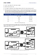
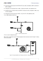
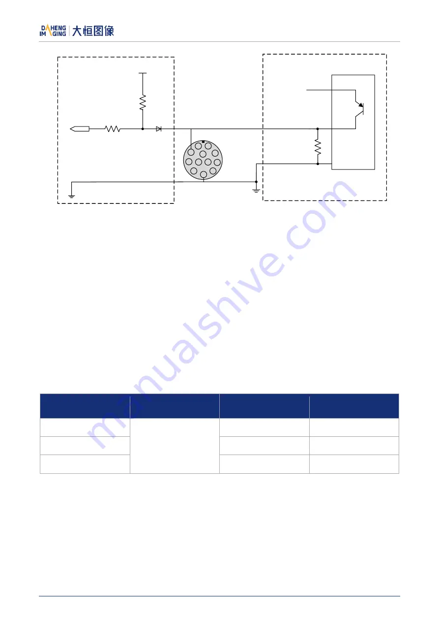
Figure 7-10 PNP photoelectric sensor connected to Line2 input circuit
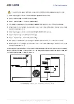
When Line2 is configured as input, if the corresponding output device is common-anode connected, pull-
down resistor over 1K should not be used, otherwise the input voltage of Line2 will be over 0.6V and logic
0 cannot be recognized stably.
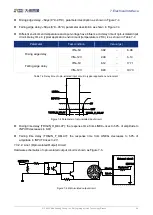
Input rising time delay: <2μs (0°C~45°C), parameter description as shown in Figure 7-4
Input falling time delay: <2μs (0°C~45°C), parameter description as shown in Figure 7-4
7.3.2.3.2.
Line2 is Configured as Output
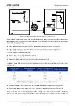
Range of external voltage (EXVCC) is 5~24V
Maximum output current of Line2 is 25mA, output impedance is 40Ω
Transistor voltage drop and output current in typical application conditions (temperature is 25
℃
) are shown
External voltage
EXVCC
External resistance
Rexternal
Transistor voltage drop
(turn on, unit V)
Output current (mA)
5V
1kΩ
0.19
4.8
12V
0.46
11.6
24V
0.92
23.1
Table 7-7 Transistor voltage drop and output current of Line2 in typical conditions
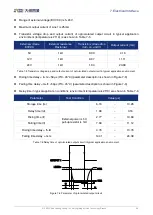
Rising time delay = tf+td: <20μs (0°C~45°C) (parameter description as shown in Figure 7-6)
Falling time delay = tr+ts: <20μs (0°C~45°C) (parameter description as shown in Figure 7-6)
Delay parameters are affected greatly by external voltage and external pull-up resistor, but little by
temperature. Output delays in typical application conditions (temperature is 25°C) are shown in Table 7-8.

