


Document type:
Title:
Revision date:
Revision:
User's Manual (MUT)
Mod. V1724 8 Channel 14bit - 100MS/s Digitizer
06/11/2007
7
NPO:
Filename:
Number of pages:
Page:
00103/05:V1724x.MUTx/07 V1724_REV7.DOC
63
51
Bits [15:0] contain the firmware revision number coded on 16 bit (X.Y format).
Example: revision 1.3 of 12
th
June 2007 is: 0x760C0103
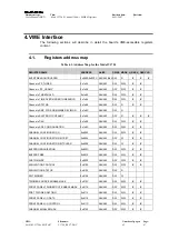
4.9.
Channel n Buffer Occupancy (0x1n94; r)
Bit
Function
[10:0] Occupied buffers (0..1024)
4.10.
Channel n DAC Register (0x1n98; r/w)
Bit
Function
[15:0] DAC
Data
Bits [15:0] allow to define a DC offset to be added the input signal in the -1.125V ÷
+1.125V range (low range) or in the -1V ÷ +8V range (high range), see also § 3.1.1.
When Channel n Status bit 2 is set to 0, DC offset is updated (see § 4.7).
4.11.
Channel n ADC Configuration (0x1n9C; r/w)
Bit
Function
[31:0] Reserved
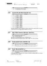
4.12.
Channel Configuration (0x8000; r/w)
Bit
Function
[19-16]
Allows to select Zero Suppression algorithm:
0000 = no zero suppression (default);
0001 = full suppression based on the integral
(ZS INT)
;
0010 = zero length encoding
(ZLE)
;
0011 = full suppression based on the amplitude
(ZS AMP)
[7]
0 = Analog monitor disabled
1 = Analog monitor disabled
[6]
0 = Trigger Output on Input Over Threshold
1 = Trigger Output on Input Under Threshold
allows to generate local trigger either on channel over or under
threshold (see § 4.3 and § 4.6)
[4]
0 = Memory Random Access
1 = Memory Sequential Access
[3]
0 = Test Pattern Generation Disabled
1 = Test Pattern Generation Enabled
[1]
0 = Trigger Overlapping Not Enabled
1 = Trigger Overlapping Enabled
Allows to handle trigger overlap (see § 3.3.4)
[0]
0 = "Window" Gate
1 = "Single Shot" Gate
Allows to handle samples validation (see § 3.3.1)
This register allows to perform settings which apply to all channels.
It is possible to perform selective set/clear of the Channel Configuration register bits
writing to 1 the corresponding set and clear bit at address 0x8004 (set) or 0x8008 (clear)
see the following § 4.13 and § 4.14. Default value is 0x10.