


Document type:
Title:
Revision date:
Revision:
User's Manual (MUT)
Mod. V1724 8 Channel 14bit - 100MS/s Digitizer
06/11/2007
7
NPO:
Filename:
Number of pages:
Page:
00103/05:V1724x.MUTx/07 V1724_REV7.DOC
63
15
2.7.
Technical specifications table
Table 2.3 : Mod. V1724 technical specifications
Package
1-unit wide VME 6U module
Analog Input
8 channels, single-ended or differential (depending on version);
2.25Vpp (10Vpp Single-ended on request) input range, positive or negative;
40MHz Bandwidth;
Programmable DAC for Offset Adjust on each channel (Single-ended versions only).
Digital Conversion
Resolution: 14 bit
Sampling rate: 10 MS/s to 100 MS/s simultaneously on each channel
Multi board synchronisation (one board can act as clock master).
External Gate Clock capability (NIM / TTL) by S_IN input connector, for burst or single sampling
mode.
ADC Sampling
Clock generation
The V1724 sampling clock generation supports three operating modes:
-
PLL mode - internal reference (50 MHz local oscillator)
-
PLL mode - external reference on CLK_IN. Frequency: 50MHz 100ppm (Other reference
frequency values are available in 10 ÷ 100MHz range.)
-
PLL Bypass mode: External clock on CLK_IN drives directly ADC clocks. External clock
Frequency from 10 to 100MHz.
CLK_IN
AC coupled differential input clock LVDS, ECL, PECL, LVPECL, CML (single ended NIM / TTL is
also possible via custom CAEN cable).
CLK_OUT
DC coupled differential LVDS output clock, locked to ADC sampling clock. Frequency values in 10
÷ 100MHz range are available.
Memory Buffer
512K sample/ch or 4M sample/ch (see § 1.1); Multi Event Buffer with independent read and write
access. Programmable event size and pre-post trigger. Divisible into 1 ÷ 1024 buffers
Trigger
Common External TRGIN (NIM or TTL) and VME Command
Individual channel autotrigger (time over/under threshold)
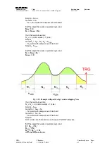
TRGOUT (NIM or TTL) for the trigger propagation to other V1724 boards
Trigger Time Stamp
32bit – 10ns (43s range). Sync input for Time Stamp alignment
AMC FPGA
One Altera Cyclone EP1C4 or EP1C20 per channel
Optical Link
Data readout and slow control with transfer rate up to 80 MB/s, to be used instead of VME bus.
Daisy chainable: one A2818 PCI card can control and read eight V1724 boards in a chain (not
available on Mod. V1724LC).
VME interface
VME64X compliant
D32, BLT32, MBLT64, CBLT32/64, 2eVME, 2eSST, Multi Cast Cycles
Transfer rate: 60MB/s (MBLT64), 100MB/s (2eVME), 160MB/s (2eSST)
Sequential and random access to the data of the Multi Event Buffer
The Chained readout allows to read one event from all the boards in a VME crate with a BLT
access
Upgrade
V1724 firmware can be upgraded via VME
Software
General purpose C Libraries and Demo Programs (CAENScope)
Analog Monitor
(not available in
V1724LC)
12bit / 100MHz DAC controlled by ROC FPGA, supports five operating modes:
-
Waveform Generator: 1 Vpp ramp generator
-
Majority:
MON/
Σ
output signal is proportional to the number of ch. under/over threshold (1 step
= 125mV)
-
Analog Inspection: data stream from one channel ADC drives directly the DAC input producing
the channel input signal (1 Vpp)
-
Buffer Occupancy: MON/
Σ
output signal is proportional to the Multi Event Buffer Occupancy:
1 buffer ~ 1mV
-
Voltage level: MON/
Σ
output signal is a programmable voltage level
LVDS I/O
16 general purpose LVDS I/O controlled by the FPGA
Busy, Data Ready, Memory full, Individual Trig-Out and other function can be programmed
An Input Pattern from the LVDS I/O can be associated to each trigger as an event marker