


Document type:
Title:
Revision date:
Revision:
User's Manual (MUT)
Mod. V1724 8 Channel 14bit - 100MS/s Digitizer
06/11/2007
7
NPO:
Filename:
Number of pages:
Page:
00103/05:V1724x.MUTx/07 V1724_REV7.DOC
63
35
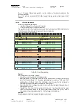
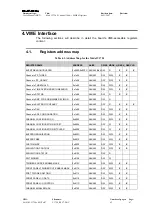
Channel sum with maximum dynamics:
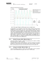
Fig. 3.18: Example of Magnify and Offset parameters use on single channel
The assumption is an input signal on CH0 using th whole dynamics and all channels
participating to Analog Monitor. The ADC on the mezzanine produces data in the
0÷16383 range (14 bit). All channels have 0 offset and therefore the ADC converted
value is 8192. The triangular waveform is shown as example. The FPGA AMC of channel
0 sends the 8 MSB to FPGA ROC with a 25 Mhz rate (one sample out of four). If no
output is added and MAGNIFY factor 1x, the DAC produces a copy of the signal on
channel 0 with 125 mV dynamics (1/8 of DAC dynamics) and 500 mV average value. If a
larger dynamics is desired, it is necessary to modify 0FFSET and MAGNIFY factor: in
order to avoid saturation it is necessary to subtract to the channel sum a value equal to
the minimum of the channel sum (displacement).
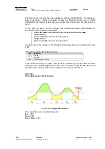
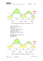
3.7.4. Buffer
Occupancy
Mode (Monitor Mode = 3)
In this mode, MON out provides a voltage value proportional to the number of buffers
filled with events; step: 1 buffer = 0.976 mV. .
This mode allows to test the readout efficiency: in fact if the average event readout
throughput is as fast as trigger rate, then MON out value remains constant; otherwise if
MON out value grows in time, this means that readout rate is slower than trigger rate.
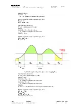
3.7.5.
Voltage Level Mode (Monitor Mode = 4)
In this mode, MON out provides a voltage value programmable via the 'N' parameter
written in the SET MONITOR DAC register, with: Vmon = 1/4096*N (Volt).