


benshaw.com
142
APPENDIX B
Table B-5-4a Terminal descriptions of RSI-PPVC-AXRY-ENPG-PG4
Table B-5-4b Indicators of RSI-PPVC-AXRY-ENPG-PG4
Figure B-5-4 Port circuit of RSI-PPVC-AXRY-ENPG-PG4
B.5.4 Resolver PG Card (RSI-PPVC-AXRY-ENPG-PG4)
Terminal
Pin
Definition
Function Description
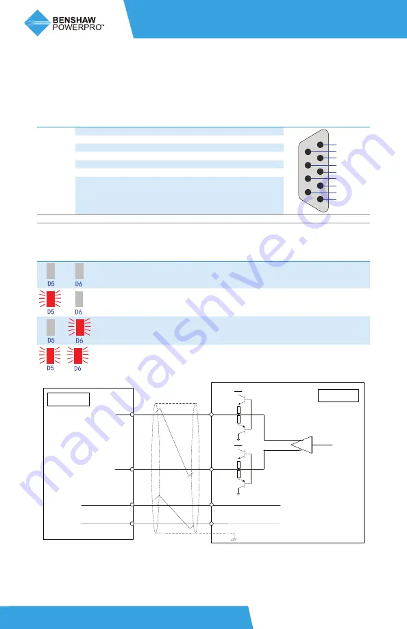
Terminal Arrangement
J3
1
EXC1
Resolver excitation negative
1
2
3
4
5
6
7
8
9
EXC1
EXC
NC
NC
SIN
NC
SINLO
COSLO
COS
2
EXC
Resolver excitation positive
3
SIN
Resolver feedback SIN positive
4
SINLO
Resolver feedback SIN negative
5
COS
Resolver feedback COS positive
6, 7, 8
NC
Vacant internally
9
COSLO
Resolver feedback COS negative
CN1
18-pin FFC interface, connecting to J4 on the control board of the AC drive
EXC
EXC1
15V
15V
SIN+/COS+
SIN-/COS-
SIN/COS
SINL0/COSL0
PE
Twisted
pair
Twisted
pair
EXC+
EXC-
PG card
Encoder
Notes: Externally excited input DC resistance must be greater than 17 Ω (can be measured
by a multimeter).Otherwise, RSI-PPVC-AXRY-ENPG-PG4 will not work normally.
It is recommended to select a resolver with a maximum of four pole-pairs.
Otherwise, RSI-PPVC-AXRY-ENPG-PG4 will be overloaded.
Indicator State
RSI-PPVC-AXRY-ENPG-PG4
Fault State
Description
Normal
None
Phase-lock loop unlocked
Phase lag of the resolver is very large.
Signal SIN/COS amplitude
exceeding the upper limit
D6 flashing is normally caused by interference. Ground the
motor well and connect the ground point of the resolver card
to PE of the drive.
Signal SIN/COS amplitude
too small
Generally, DB9 is not connected or not properly connected,
or wire is broken. If the preceding conditions do not occur,
check whether the resolver model selection is correct or not.


