background image

14

Avago Technologies Confidential

Control Interface

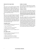
The control interface includes a bi-directional Int_L/

Reset_L interrupt/reset signal and two-wire serial – SCL 

(clock) and SDA (data) signals to provide users rich func-

tionality over an efficient and easily used interface. The 

TWS interface is implemented as a slave device and com-

patible with industry standard two-wire serial protocol. 

Signal and timing characteristics are further defined in 

this section. In general, TWS bus timing and protocols 

follow the implementation popularized in Atmel Two-wire 

Serial EEPROMs. 

Low-Speed Electrical Contact Definitions


SDA, SCL

SCL is the clock of the two-wire serial interface, and SDA is 

the data for the two-wire interface. SCL and SDA must be 

pulled up in the host through a pull-up resistor of value 

appropriate to the overall bus capacitance and the rise 

and fall time requirements as per “CXP two-wire Serial 

Interface Timing Specifications” table.
The host supplied SCL input to the CXP transceiver is used 

to positive-edge clock data into each CXP device and neg-

ative-edge clock data out of each device. CXP transceivers 

operate only as slave devices. The host must provide a bus 

master for SCL and initiate all read/write communication.
Since all CXP transceivers use the same two base 

addresses, each CXP port requires its own SCL/SDA bus. 

Support of multiple ports in a host requires multiple SCL/

SDA buses, or multiplexing circuitry such as a multiplexer 

chip or a switch chip.

INT_L/RESET_L

Int_L/Reset_L is a bidirectional contact. When driven 

from the host, it op erates logically as a Reset signal. 

When driven from the module, it oper ates logically as an 

Interrupt signal. In both cases, the signal is asserted low, 

as indicated by the ’_L’ suffix. The Int_L/Reset_L signal 

requires open collector outputs in both the host and  

the module, and must be pulled up on the host board 

with 1.5 kohm – 10 kohm resistor. The two uses are  

distinguished by timing – a shorter assertion, driven by 

the module indicates an interrupt and a longer assertion 

of the signal driven by the host indicates a reset as per “I/O 

Timing for Control and Status Functions” Table below.

Int_L operation: 

When Int_L/Reset_L is pulled “Low” by the module for 

longer than the minimum pulse width (t

Int_L, PW-min

) and 

shorter than the maximum pulse width (t

Int_L, PW-max

) the 

signal signifies an interrupt. When asserted “Low”, Int_L 

indicates a possible module operational fault or a status 

critical to the host system. The host identifies the cause 

of the interrupt using the two-wire serial interface. Int_L 

must operate in Pulse mode (as opposed to Static mode), 

in order to distinguish a short Int_L signal from a longer 

Reset_L signal, so the module must de-assert Int_L/

Reset_L after the interrupt has been signaled.

Reset_L operation: 

When the Int_L/Reset_L signal is pulled “Low” by the 

host for longer than the minimum reset pulse length 
(

t

Reset_L,PW-min

), it ini tiates a complete module reset, 

returning all user module settings to their default state. 

There is no maximum reset pulse length. Module Reset 

Assert Time (t_init) starts on the rising edge after the 

low level on the Reset_L signal is released. During the 

execution of a reset (t_init) the host shall disregard all 

status bits until the module indicates a completion of the 

reset interrupt. The module indicates this by posting an 

Int_L signal with the Data_Not_Ready bit (Memory Map, 

Byte 2, bit 0) negated. Note that on power up (including 

hot insertion) the module will post this completion of 
reset interrupt without requiring a reset from the host. 

PRSNT_L 

PRSNT_L is used to indicate when the module it plugged 

into the host re ceptacle. PRSNT_L is pulled up to Vcc3.3 

on the host board through > 50 k

W

 and pulled down 

directly to signal common (no re sistor) in the module. The 

PRSNT_L is asserted “Low” when inserted and deas serted 

“High” when the module is physically absent from the host 

con nector. 

Summary of Contents for AFBR-83CDZ

Page 1: ...ght weight cable management Description The Avago Technologies AFBR 83CDZ is a Twelve Chan nel Pluggable Parallel Fiber Optic CXP Transceiver for 12 12 5G proprietary application This transceiver is a...

Page 2: ...100 Ohms AC coupling capacitors are located inside the CXP module and are not required on the host board For module control and inter rogation the control interface incorporates a Two Wire Serial TWS...

Page 3: ...ontrol Rx Output de Emphasis Control Four bit code blocks bits 7 4 or 3 0 are assigned to each channel Codes 1xxxb are reserved Writing 0111b calls for full scale de emphasis Writing 0000b calls for m...

Page 4: ...Voltage Single Ended 0 5 Vcc33 0 5 4 0 V Data Input Voltage Differential Vdip Vdin 1 6 V Note 2 Control Input Voltage Vi 0 5 Vcc33 0 5 4 0 V Note 3 Control Output Current Io 20 20 mA Relative Humidity...

Page 5: ...h 2000 MHz km 50 m MMF OM3 50 m Receiver Differential Data Output Load 100 W Note 1 For applications other than 12 5 Gbps per channel please contact Avago Sales 2 Per IEEE 802 3ba 2010 TP1a and TP4 CP...

Page 6: ...Jitter tolerance TP1a 0 25 UI DJ Jitter tolerance TP1a 0 15 UI RJ Jitter tolerance TP1a 0 10 UI Data Dependent Pulse Width Shrinkage DDPWS tolerance TP1a 0 07 UI Eye Mask Coordinates X1 X2 Y1 Y2 TP1a...

Page 7: ...TP4 0 75 UI DJ Jitter output TP4 0 45 UI RJ Jitter output TP4 0 30 UI Data Dependent Pulse Width Shrinkage DDPWS TP4 0 34 UI Eye Mask coordinates X1 X2 Y1 Y2 TP4 SPECIFICATION VALUES 0 29 0 5 110 425...

Page 8: ...65 nm RMS Spectral Width is the standard deviation of the spectrum Average launch power each lane TP2 7 6 2 4 dBm Optical Modulation Amplitude OMA each lane TP2 5 6 3 dBm Even if the TDP 0 9 dB the OM...

Page 9: ...tter each lane TP3 0 47 UI OMA of each aggressor lane TP3 0 4 dBm Rx LOS Assert Threshold TP3 30 dBm OMA Rx LOS De assert Threshold TP3 8 dBm OMA LOS Hysteresis TP3 0 5 dB Notes 1 The receiver shall b...

Page 10: ...z applied to the module without a chassis enclosure Laser Eye Safety and Equipment Type Testing EN 60950 1 2006 A11 A1 A12 EN 60825 1 2007 EN 60825 2 2004 A1 A2 Pout EN AEL US FDA CDRH Class 1M TUV Fi...

Page 11: ...GND D7 C8 Rx5p Rx4p D8 C9 Rx5n Rx4n D9 C10 GND GND D10 C11 Rx7p Rx6p D11 C12 Rx7n Rx6n D12 C13 GND GND D13 C14 Rx9p Rx8p D14 C15 Rx9n Rx8n D15 C16 GND GND D16 C17 Rx11p Rx10p D17 C18 Rx11n Rx10n D18...

Page 12: ...L I A19 GND Ground A20 SCL Two wire serial interface clock LVCMOS I O 1 A21 SDA Two wire serial interface data LVCMOS I O 1 B1 GND Ground B2 TX0p Transmitter Non Inverted Data Input CML I B3 TX0n Tran...

Page 13: ...a Output CML O D3 RX0n Receiver Inverted Data Output CML O D4 GND Ground D5 RX2p Receiver Non Inverted Data Output CML O D6 RX2n Receiver Inverted Data Output CML O D7 GND Ground D8 RX4p Receiver Non...

Page 14: ...ed up on the host board with 1 5 kohm 10 kohm resistor The two uses are distinguished by timing a shorter assertion driven by the module indicates an interrupt and a longer assertion of the signal dri...

Page 15: ...dule returns to the factory default control settings While Reset_L is low the Tx and Rx outputs are disabled and the module does not response to the 2WS serial interface 5 Time from power on to Data N...

Page 16: ...0 3 V Condition IOL 3 0 mA Pull up to 3 3V Module Output Voltage High Voh 2 8 3 6 V Min Voh 3 3V 0 5V Module Output Current High Ioh 10 10 A 0 3 V Voutput 3 6 V Capacitance of module on SCL SDA and I...

Page 17: ...SDA or Vih min SDA 4 Rise Time is measured from Vol max SDA to Voh min SDA 5 Fall Time is measured from Voh min SDA to Vol max SDA Memory Specifications Memory may be accessed in single byte or multi...

Page 18: ...s reached 2 Time from resumption of Rx input signals until normal Rx output condition is reached 3 Time from loss of Tx input signal until the squelched output condition is reached 4 Time from resumpt...

Page 19: ...ax Case Temp Min Max Signal Rate Laser Wavelength or Copper Attenua tion and Supported Functions 147 RO Description Device Technology 152 222 RO Vendor Information Name OUI PN PN rev Serial Number Dat...

Page 20: ...wn so that the helix half twist incurred when the cable is lugged into transceivers will correctly connect transmitter lanes to receiver lanes lanes 0 to 0 and 11 to 11 MPO style male alignment pins a...

Page 21: ...go Technologies Confidential Mechanical Dimensions Package Outline Figure 10 Transceiver package dimensions All dimensions in millimeters 48 62 13 73 7 69 9 81 23 9 4 6 112 67 92 28 45 19 21 34 93 23...

Page 22: ...Co 0 05 0 05 AD03 Latch Hole Width 1 50 0 10 AD11 Locating Post to EMI Shell Base 18 06 0 13 AD04 Datum to Latch Hole 5 40 0 10 AD12 Locating Post to Face 25 06 0 08 AD05 Latch Hole to Hole 10 80 0 05...

Page 23: ...m Tol AE01 Orientation Key Location 1 63 0 13 AE07 Snout Height 11 70 0 08 AE02 Orientation Key Location Depth 20 75 Basic AE08 Snout Opening Height 10 20 0 05 AE03 Card Slot Height 1 18 0 05 AE09 Rec...

Page 24: ...ocating Hole to First Row of Signal Holes 0 20 Basic AK08 Contact Hole Diameter Finished PTH 0 37 0 05 AK03 First Row to Second Row of Signal Holes 0 70 Basic AK09 Row A to Row B 4 00 Basic AK04 First...

Page 25: ...EMI Shell 19 66 Basic AJ02 Bezel Opening Figure 15 CXP bezel opening dimensions ID Description Dim Tol ID Description Dim Tol AH01 Cutout Height 12 10 Basic AH03 Bottom of Cutout to Peg 0 28 Basic AH...

Page 26: ...er Min Max Unit Comments Fi CXP module insertion force 150 N EIA 364 13 Fw CXP module extraction 50 N EIA 364 13 Fr CXP module retention 90 170 N Load pull per EIA 364 38A No damage to transceiver bel...

Reviews: