VC707 Evaluation Board
55
UG885 (v1.2) February 1, 2013
Feature Descriptions
•
2 differential clocks
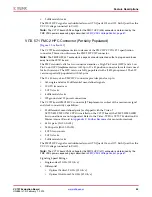
The FMC1 HPC signals are distributed across GTX Quads 118 and 119. Each Quad has the
VCCO voltage connected to VADJ.
Note:
The VC707 board VADJ voltage for the FMC1 HPC (J35) connector is determined by the
FMC VADJ power sequencing logic described in
FMC_VADJ Voltage Control, page 67
VITA 57.1 FMC2 HPC Connector (Partially Populated)
[
, callout
The VC707 board implements two instances of the FMC HPC VITA 57.1 specification
connector. This section discusses the FMC2 HPC J37 connector.
Note:
The FMC2 HPC J37 connector is a keyed connector oriented so that a plug-on card faces
away from the VC707 board.
The FMC standard calls for two connector densities: a High Pin Count (HPC) and a Low
Pin Count (LPC) implementation. A 400 pin 10 x 40 position connector form factor is used
for both versions. The HPC version is fully populated with all 400 pins present. The LPC
version is partially populated with 160 pins.
The 10 x 40 rows of an FMC HPC connector provides pins for up to:
•
160 single-ended or 80 differential user-defined signals
•
10 GTX transceivers
•
2 GTX clocks
•
4 differential clocks
•
159 ground and 15 power connections
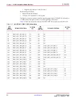
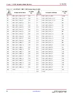
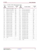
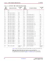
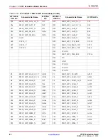
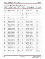
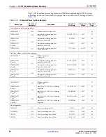
The VC707 board FMC2 HPC connector J37 implements a subset of the maximum signal
and clock connectivity capabilities:
•
58 differential user-defined pairs (as shipped with the Virtex-7
XC7VX485T-2FFG1761C FPGA installed on the VC707 board, the FMC2 HB00-HB21
bus connections are not supported. Refer to the Virtex-7 FPGA VC707 Evaluation Kit
Master Answer Record in
:
for more information).
•
34 LA pairs (LA00-LA33)
•
24 HA pairs (HA00-HA23)
•
8 GTX transceivers
•
2 GTX clocks
•
2 differential clocks
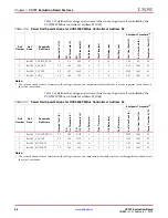
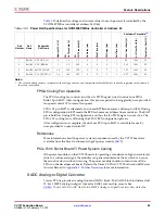
The FMC2 HPC signals are distributed across GTX Quads 116 and 117. Each Quad has the
VCCO voltage connected to VADJ.
Note:
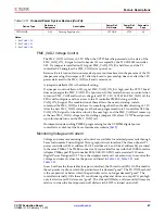
The VC707 board VADJ voltage for the FMC2 HPC (J37) connector is determined by the
FMC VADJ power sequencing logic described in
FMC_VADJ Voltage Control, page 67
Signaling Speed Ratings:
•
Single-ended: 9 GHz (18 Gb/s)
•
Differential
•
Optimal Vertical: 9 GHz (18 Gb/s)
•
Optimal Horizontal: 16 GHz (32 Gb/s)
Содержание VC707
Страница 1: ...VC707 Evaluation Board for the Virtex 7 FPGA User Guide UG885 v1 2 February 1 2013...
Страница 74: ...74 www xilinx com VC707 Evaluation Board UG885 v1 2 February 1 2013 Chapter 1 VC707 Evaluation Board Features...
Страница 94: ...94 www xilinx com VC707 Evaluation Board UG885 v1 2 February 1 2013 Appendix D Board Setup...
Страница 96: ...96 www xilinx com VC707 Evaluation Board UG885 v1 2 February 1 2013 Appendix E Board Specifications...

