10
VC707 Evaluation Board
UG885 (v1.2) February 1, 2013
Chapter 1:
VC707 Evaluation Board Features
Each configuration interface corresponds to one or more configuration modes and bus
widths as listed in
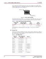
. The mode switches M2, M1, and M0 are on SW11 positions 3,
4, and 5 respectively as shown in
.
The default mode setting is M[2:0] =
010
, which selects Master BPI at board power-on. See
Configuration Options, page 71
for detailed information about the mode switch SW11.
For full details on configuring the FPGA, see
7 Series FPGAs Configuration
User Guide
.
I/O Voltage Rails
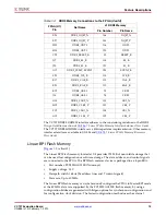
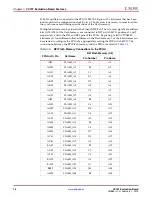
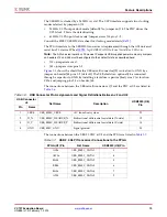
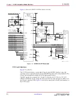
There are 17 I/O banks available on the Virtex-7 device. Sixteen I/O banks are available on
the VC707 board, bank 31 is not used. The voltages applied to the FPGA I/O banks used by
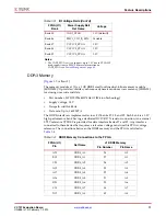
the VC707 board are listed in
X-Ref Target - Figure 1-3
Figure 1-3:
SW11 Default Settings
Table 1-2:
VC707 Board FPGA Configuration Modes
Configuration
Mode
SW13 DIP switch
Settings (M[2:0])
Bus
Width
CCLK
Direction
Master BPI
010
x8, x16
Output
JTAG
101
x1
Not Applicable
UG885_c1_03_020612
1
OFF Position = 0
ON Position = 1
2 3 4 5
A25
A24
M2
M1
M0
Table 1-3:
I/O Voltage Rails
FPGA (U1)
Bank
Power Supply Rail
Net Name
Voltage
Bank 0
VCC1V8_FPGA
1.8V
Bank 13
VCC1V8_FPGA
1.8V
Bank 14
VCC1V8_FPGA
1.8V
Bank 15
VCC1V8_FPGA
1.8V
Bank 16
VADJ_FPGA
1.8V (default)
Bank 17
VADJ_FPGA
1.8V (default)
Bank 18
VADJ_FPGA
1.8V (default)
Bank 19
VADJ_FPGA
1.8V (default)
Bank 31
NOT USED
NA
Bank 33
VCC1V8_FPGA
1.8V
Bank 34
VADJ_FPGA
1.8V (default)
Содержание VC707
Страница 1: ...VC707 Evaluation Board for the Virtex 7 FPGA User Guide UG885 v1 2 February 1 2013...
Страница 74: ...74 www xilinx com VC707 Evaluation Board UG885 v1 2 February 1 2013 Chapter 1 VC707 Evaluation Board Features...
Страница 94: ...94 www xilinx com VC707 Evaluation Board UG885 v1 2 February 1 2013 Appendix D Board Setup...
Страница 96: ...96 www xilinx com VC707 Evaluation Board UG885 v1 2 February 1 2013 Appendix E Board Specifications...


