background image

4-3 . 

PERFORMANCE TESTS 

The  fol lowing  Performance Tests  are  procedures whi ch can be  used  to veri fy 

that  the  instrument is operating  properly and meets the  specifi cations  l isted 

below .  A l l  speci fi cations  apply  to  Butterworth  (Flat Ampl . )  response and  al l 

Performance  Tests  are  performed with  the  Flat Ampl ./Flat De l ay  switch  in the 

F l at Amp! .  position . 

Parameter 

Passband Gain Accuracy 

Cutoff Frequency Calibration 

A ccuracy 

D C  Offset 

Broadband  Noise 

Maximum Stopband Attenuation* 

Harmonic Components' 

AC  Line-related Spurious 

Components' 

S pecification 

Model  452 

0 ±0 . 25 dB, 
20 ±0. 25 dB 

(±0 . 5  dB, H P, x1 0K) 

±2% 

0±2 .5  mV  de 

1 00  uV  rms,  max . 

90 dB 

-90 dB 

-1 1 0 dB 

relative to ful l -scale signal  of 7 . 1  V  rms  ( +1 7  dBV) 

a .  

Passband Gain 

(  See  Fig.  4-3) 

Model  852 

±0.5 dB , 

20 ±0. 5  dB 

(±l dB , H P, x 1 0K )  

±2% 

±2 . 5  mV  de 

200 uV rms,  max. 

90 dB 

-80 dB 

-1 00 dB 

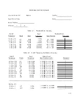
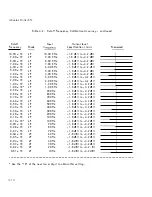
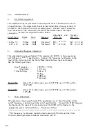
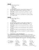
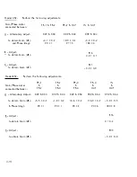
Connect equipment as shown  in Setup #1 .   Set Frequency Synthesizer output 
to 0 . 7 1  V  rms and measure  possband gain of the Channel  Under Test  (CUT) 

for the settings shown in Table 4 . 1 .  

4-5 

Содержание 452

Страница 1: ...frequency domain applications and Flat Delay response for transient free time domain applications The Models 452 and 852 are elec trically and mechanically similar each covering the cutoff frequency...

Страница 2: ...Between Channels Typical 452 452 01 1 or 1 whichever is greater 852 852 01 2 or 2 whichever is greater FLAT DELAY RESPONSE Low Pass Delay Typical 452 452 01 1 2fc sec 852 852 01 1 fc sec Attenuation...

Страница 3: ...IS PROVIDED SOLELY FOR INSTRUMENT OPERATION AND MAINTENANCE THE INFORMATION IN THIS DOCUMENT MAY NOT BE DUPLICATED IN ANY MANNER WITHOUT THE PRIOR APPROVAL IN WRITING FROM WAVETEK W AVETE WAVETEK SAN...

Страница 4: ...plier I anges Page 1 6 Paragraph 1 5 following Frequency Range table bottom of page Add NOTE Specifications apply for cutoff frequency dial settings from 0 10 to 10 1010 Page 1 7 PaI agI aph 1 5 Maxim...

Страница 5: ...Buyer shall prepay shipping charges taxes duties and insurance for products returned to Wavetek for warranty service Except for products returned to Buyer from another country Wavetek shall pay for re...

Страница 6: ...covers removed This should be done only by qualified personnel aware of the electrical hazards The instrument power receptacle is connected to the instrument safety earth terminal with a green yellow...

Страница 7: ...ay for frequencies below its cutoff frequency This fil ter is suitable for time domain applications because of its inherent obil ity to poss transient waveforms with a very sma l l amount of d istorti...

Страница 8: ...nts It is 1 3 inches deep and weighs 1 0 pounds Model 452 or 1 2 pounds Model 852 The power switch operating controls and input and output terminals are located on the front panel The rear panel conta...

Страница 9: ...1 0 and a four position xl 0 xl 00 xl K xl 0K multiplier switch Option 01 adds a fifth position x1 to the multiplier switch Multiplier xl xl 0 xl 00 xl K x l 0K Frequency Hz 0 01 1 1 1 0 1 1 1 1 l l...

Страница 10: ...is greater FLAT DELAY RESPONSE Low Pass Delay Typical Attenuation at Cutoff S tabil ity of Delay Typical Phase Match between Channels Typical INPUT CHARACTERISTICS Circuit Impedance F ul l scal e Sig...

Страница 11: ...purious Companents 110 dB below ful l scale signal DC Offset at 25 C Within 2 5 m i l l ivolts at any fc setting Drift vs Temperature 100 microvolts oC typ 500 micravolts oC max Drift vs Time Typical...

Страница 12: ...ass Two channels connected in parall e l Low Pass DC Coupled with 48 dB oct rol loff High Pass with 48 dB oct rol loff Low Pass with 96 dB oct roll oH High Pass with 96 dB oct rol loff B and Pass with...

Страница 13: ...2 fc and is equal to 0 22 f Band Reiect An insertion loss of approximately 6 dB is produced Cutoff Frequency Accuracy 2 Attenuation at Cutoff 3 dB Stopband Attenuation Rate Rol loff 48 dB octave nomi...

Страница 14: ...V rms DC to 300 KHz decreasing to 4 Volts 2 8 V rms at 1 MHz R 2 5 K 1 5 mA max current L Broadband Noise at either Gain Setting 200 microvolts rms max for 1 00 KHz detector bandwidth Harmonic Compon...

Страница 15: ...Size Weight Configuration Accessories supplied 1 1 5 230 VAC 1 0 10 50 500 Hz S walts BNC s on front rear panel S lide switch on rear panel to disconnect circuit ground from power ground 3 1 2 H x 1...

Страница 16: ......

Страница 17: ...laim with the carrier immediatel y Preserve the carton and packing materials they wil l be required by the carrier It is recommended that conformance to specifications be verified upon receipt In case...

Страница 18: ...ack mount brackets are to prevent the instrument from sliding when mounted in a rack They are not intended to support the weight of the instrument and should never be used for lifting or carrying Inst...

Страница 19: ...lel ground adapter and connect the short lead to ground 2 4 CONTROLS AND I ND ICATORS Controls and indicators are shown in Figure 2 1 and described i n Table 2 1 The descriptions i n Table 2 1 and the...

Страница 20: ...gh Pass Out selector switch Output BNC Connector F lat Delay In or F l at Amplitude Out selector switch 20 dB Gain In or 0 dB Gain Out selector switch Input BNC Connector Channel 2 Controls and Indica...

Страница 21: ...1 2 3 4 5 11 10 9 12 13 14 19 6 7 FRONT PANEL 8 15 16 REAR PANEL Figure 2 1 Controls and Indicators 17 18 2 5...

Страница 22: ...tion is due to Siew Rate limitations of the Operational Amplifiers employed in the instrument When 20 dBGC l in Volt 0 71 V 10 8 6 CAUTION Input signals i n Gain setting may damage the instrument t 4...

Страница 23: ...response ral ls off at a rate of24 dB octave 8 and48 dB octave 160 The Low Pass or High Pass Butterworth response for either model may be deter mined by Icaling the normalized plots given in Figures2...

Страница 24: ...a vailable at OUT 2 The passband in this configuration extends from the High Pass Cutoff Frequency to the Low Pass Cutoff Frequency setting Maximum passband gain of 40 dB is available If only 20 dB g...

Страница 25: ...ends from the Low Pass Cutoff Frequency to the High Pass Cutoff Frequency Again the overa l l response may be determined by combining the normal ized plots given in Figures 2 3 through 2 6 f Sharp Not...

Страница 26: ...ow the reduction in input signal shown in Fig 2 2 provided the current required by the load connected to the instrument does not exceed the maximum value of 15 mAo Heavy capacitive l oads can easily...

Страница 27: ...tI W III 2 0 11 2 Ul W II 3 0 2 t m Ul Ul a 1 2 1 0 o m tI 20 W Ul 2 o 40 11 Ul W II 60 o 2 3 4 5 6 B 2 3 4 5 6 NORMALIZEO FREGlUENCY E Fe Fig 2 3 452 Flat Ampl Respanse La Pas BO t m 11 o 100 I B 10...

Страница 28: ...1 2 BP 3SNOdS3t f CN f8SS fd o N I I I I I 1 0 III W 10 u l U N 2 w J c J w II Il C III w N W oJ 10 ct II C 2 N o N o w o III O o o I I I I I C BP 1 3SNOdS3t f CN fBdO LS 0 I c 0 E 0 u N l t t I N OJ...

Страница 29: ...0 o W 1 III 2 0_2 11 III W II 3 o 2 m III III 1 2 I I 1 i I 3 4 5 6 S 1 2 3 4 5 6 NORMALIZED FREQUENCY Fe Fig 2 5 852 Flat Amp Response Lo Pass o m 0 20 W Ul 2 o 40 11 Ul w 60 II o 2 so m 11 o 100 l S...

Страница 30: ...o m 0 0 W 1Il 20 2 o 0 40 III w a 0 60 2 m BO 0 o I 111 100 1 2 I 3 4 5 6 B 1 2 3 4 5 6 NORMALIZEO FREGUENCyeL Fe Fig 2 6 852 Flat Ampl Response Hi Pass o m 0 1 W III 2 3 2 o 0 III w a o 2 m III III B...

Страница 31: ...8 ttl 6 J W o 4 o 2 J eX 0 0 II o 2 FL AT A IPL FLA CELt Y f t 2 4 6 8 1 0 1 2 1 4 1 6 1 8 NO MALIZEO F EGUENCY Fe Fig 2 7 452 Phase Response Lo Pass I FLA AMF r FLA CEL Y L t 2 4 6 8 1 0 1 2 1 4 1 6...

Страница 32: ...2 2 J W o 13 o 2 1 6 W 4 N J c a a tI o 2 K FLA AMPi FLAT CEL 2 4 6 13 1 0 1 2 1 4 1 6 1 13 NORMALIZED FREGUENCY Fe Fig 2 9 852 Phase Response Lo Pass I FLA AMI r FLA 1 CELJ Y 2 4 6 13 1 0 1 2 1 4 1...

Страница 33: ...SS f V V FILTER WHIGH PASS I K FILTER DETERMlNES Ie Band Reject Filter 80TH FILTERS SET AT fc LOW PASS f LOW A S FILTER FILTER TPUT Low Pass Filter with Doubled Rolioff Fig 2 11 PASSBAND t cI2 Ie 2 ll...

Страница 34: ...N Xl o 3 6 m 20 11 o J W g 40 I J D SO ao 100 r I 1 1 1 I I f 1 1 r I 1 I I 0 1 02 04 08 I 2 4 8 2 4 8 10 20 40 80 NORMAL IZEO FREQUENCY _ F C Fig 2 12 452 Sharp Notch Response...

Страница 35: ...as a building block to synthesize higher order fi lters The gains of these stages at dc and at cutoff are as fol lows Input Attenuator Input Buffer 1 st Prototype 2nd Prototype Overal l OUT IN Gain a...

Страница 36: ...3 0 dB Cutoff Freguency control is obtained by changing the resistors of the filter i n 8 4 2 1 BCD steps The capacitors are changed i n decade steps and Option 01 adds an extra set of capacitors to...

Страница 37: ...SS FLAT AMPL FLAT DELAY I r L ___ I I I I TP 2 I 1sl 2nd 2nd ORDER 2nd ORDER BUFFER PROTOTYPE PROTOTYPE CHANNEL 1 MAINBOARD ASS Y 0 15V OPTIeN 01 ASS Y POWER Channell SUPPLY ASS Y OPTION 01 ASS Y Chan...

Страница 38: ...I I I c TP I I TP 2 I TP 3 I t 2nd 3rd 1 4 2nd ORDER 1 9 2nd ORDER t L l 2nd ORDER PROTOTYPE PROTOTYPE PROTOTYPE CHANNEL 1 MAINBOARD ASS Y 0 15V OPTION 01 ASS Y POWER Channell SUPPLY ASS Y OPTION 01...

Страница 39: ...de of such prototype sections may be tailored by appropriate selection of damping and the desired higher order filter may thus be synthesized In the Model 452 a fourth order Flat Amplitude or Butterwo...

Страница 40: ...w CJ 20 10 co 0 UJ VI Z 0 0 0 V1 UJ UJ Cl 10 J a E 20 30 1 2 3 4 5 6 8 1 2 3 4 5 N ORMALIZED FREQUENCY FIFe Fig 3 4 Response of 2nd order low Pass Prototype for various values of damping B 6 8 10...

Страница 41: ...Digital Multimeter 1 00 uV de resolution AC Voltmeter 1 accuracy RMS Voltmeter True RMS Frequency Synthesizer 70 dB harmonics at 1 K Hz Bond Pass Filter 24 dB oct rolloff 40 dB Gain Spectrum Analyzer...

Страница 42: ...components 1 1 5 9 K Fig 4 1 1 KHz Notch Fi lter WAR N I N G The specifications of these i nstruments cannot be veri fied unl ess the recommended equi pment or equa l is uti l ized i n test In particu...

Страница 43: ...50 ohm CUT r 5K Setup 1 452 CUT B P Filter Setup 2 50 ohm I C UT r 5K Setup 3 50 f LPF I CUT ohm 400FL Notch AC Voltmeter Filter Setup 4 Fig 4 2 Performance Test Setups b 400FL AC Voltmeter 3620A RMS...

Страница 44: ...r Top figures Figures in parentheses 452 Specifications 852 Specifications Ideal Respoose r fc 2 fc Specification Limits Effect of Passband I Frequency Tolerance Fig 4 3 Passband Gain Cutoff Frequency...

Страница 45: ...tion Accuracy D C Offset Broadband Noise Maximum Stopband Attenuation Harmonic Components AC Line related Spurious Components S pecification Model 452 0 0 25 dB 20 0 25 dB 0 5 dB H P x1 0K 2 0 2 5 mV...

Страница 46: ...the input connector of the Channel Under Test CUT and the DC Multimeter across the output connector A l l ow at least 1 0 minutes for the i nstrument to warm up under its own power and measure the DC...

Страница 47: ...off Frequency H i Pass 20 dB Gain F lat Ampl Set the 51 00 Frequency Synthesizer to 1 00 KHz and increase its output amplitude until CUT output is equal to ful l scal e signal of 7 1 V nms 1 7 dBV Set...

Страница 48: ...of 1 00 x l K 0 dB Gain Flat Ampl response Set the Channel Under Test as fol l ows 1 00 x 1 0 Cutoff Frequency Hi Pass 20 dB Gain Flat Ampl Increase Synthesizer amplitude unti l ful l scale signal of...

Страница 49: ...as fol lows 1 0 00 x 1 0 K Cutoff Frequency Lo Pass o dB Gain F lat Ampl Set the 3580A S pectrum Analyzer controls as fol lows Input Sensitivity 30 dBV Input Sensitivity Vernier CAL Bandwidth 3 Hz Fre...

Страница 50: ...band Gain Gain Frequency S pecification o dB 1 KHz o 25 dB 20 dB 1 K Hz 20 25 dB o dB 1 0 K Hz o 25 dB 20 dB 1 0 KHz 20 25 dB o dB 1 00 KHz o 5 dB 20 dB 1 00 K Hz 20 5 dB Table 4 2 Cutoff Frequency Ca...

Страница 51: ...P 900 Hz 2 40 dBY to 3 60 dBY 0 80 x 1 K L P 800 Hz 2 40 dBY to 3 60 dBY 0 70 x l K L P 700 Hz 2 40 dBY to 3 60 dBY 0 60 x 1 K LP 600 Hz 2 40 dBY to 3 60 dBY 0 50 x 1 K L P 500 Hz 2 40 dBY to 3 60 dB...

Страница 52: ...dB H P 2 0 dB Table 4 4 Mode Gain LP o dB L P 2 0 dB H P o dB H P 2 0 dB D C Offset Specification 2 5 mV dc 2 5 mV dc 2 5 mV d c 2 5 mV dc Broadband Noise Specification 1 00 uV rms max 1 00 uV rms max...

Страница 53: ...able 4 1 Passband Gain Accuracy Input Passband Gain Gain Frequency Specification o dB 1 K Hz o 5 dB 20 dB 1 K Hz 20 5 dB o dB 1 0 K Hz o 5 dB 20 dB 1 0 K Hz 20 5 dB o dB 1 00 K Hz O 1 dB 20 dB 1 00 KH...

Страница 54: ...Hz 1 8 dBV to 4 2 dBV l P 5 00 KHz 1 8 dBV to 4 2 dBV l P 4 00 KHz 1 8 dBV to 4 2 dBV l P 3 00 KHz 1 8 dBV to 4 2 dBV L P 2 00 KHz l B dBV to 4 2 dBV L P 1 00 KHz l B dBV to 4 2 dBV L P 1 00 KHz 1 8 d...

Страница 55: ...2 0 dB 200 uY rms max 0 01 x 1 0 H P o dB 200 uY rms max 0 01 x 1 0 H P 20 dB 200 uY rms max Table 4 5 Maximum Stopband Attenuation Cutoff Input Frequency Mode Frequency Specification 1 00 x 1 0K L P...

Страница 56: ...dB gain is out of specifi cation Connect the Frequency Synthesizer to the input of the instrument and the Gain Phase Meter betwen input and output Use the fol l owing settings Input Frequency Amplitud...

Страница 57: ...t R1 9 to obtain a reading of 1 7 4 dBV 5 Move the AC Voltmeter to T P 4 and adjust R24 to obtain a reading of 1 2 8 dBY 6 Move the AC Voltmete to OUT and adjust R31 to obtain a reading of 3 6 dBV 7 C...

Страница 58: ...9 3 0 2 90 3 Model 852 Perform the fol lowing adjustments TP l TP 2 TP 3 Gain Phase meter connected between T P 2 TP 3 T P 4 Alternately Adjust C29 C34 C39 C44 C49 C54 to obtain Gain dB 5 5 0 2 1 9 0...

Страница 59: ...n switch by verifying a short open between the third wire of the power cord and the she l l of one of the BNC connectors If one LED indicator is on and the other is off troubleshoot the Power Supply b...

Страница 60: ...ply leads from Mainboard Turn on instrument and measure 1 5 V dc and 15 V dc at these leads Yes Turn off instrumen and reconnect leads to Main baard Turn on instrument and al low 1 0 minutes warm up T...

Страница 61: ...e Shield Box forward c Remove the four screws which fasten the Power Supply board to the Rear Panel standoffs Disconnect Power Supply leads from Mainboards and move Power Supply board out of the Shiel...

Страница 62: ...ce CR1 8 C7 points marked I 0 Yes V Measure 1 5 V de 15 Y dc No O 25 Y de at left set of points Replace U2 marked 1 5 15 point marked o is ground Yes Measure 1 5 Y de 15 Y dc No O 25 Y de at right set...

Страница 63: ...t i s required access to the bottom of the Mainboard is either readi ly available or if behind one of the Support B ars it may be made avai lable as fol lows a Remove the three screws from each Mainbo...

Страница 64: ...dBV at OUT N o I Replace AR3 Model 452 Measure 1 6 6 dBV at TP 1 Na I Replace AR1 I Yes Measure 1 6 3 dBV at TP 2 N o Replace AR2 Yes Measure 1 3 8 dBV at TP 3 N o Replace AR3 Yes Measure 8 3 dBV at...

Страница 65: ...h of the cut pins or l eads and remove from the board clean the hol e s with a toothpick or solder suction tool Form the tinned l eads of the replacement part and insert in the printed circuit holes s...

Страница 66: ...the powe r s u ppl y s h i el d p ry out the b l ack Hayco grommet Cut any cab l e t i es i f n e ede d Step 7 R emove the two sc rews ho l di ng the rea r pa n el to s i de frame a nd t he two sc re...

Страница 67: ...ddress inqui ry to your Wavetek Representative or Wavetek San Diego Inc 9045 Balboa Ave San Diego CA 921 23 Phone 61 9 279 2200 TWX 91 0 355 2007 Specify the fol lowing information A AR B C CR DS F FL...

Страница 68: ...t 500 uF 50 V C Fxd tant 0 01 uF 20 35 V C Fxd polyester 0 001 5 uF 1 0 1 00 V CR S i l FWB 50 PIV 1 5 A R Fxd camp 1 5K 5 1 4W R Fxd comp l 0 ohm 5 1 4W R Fxd comp 2 2K 5 1 4W S Switch S lide DPDT PC...

Страница 69: ...etflm 900K 1 l SW R Fxd metflm l OOK 1 1 SW R Fxd comp 2 7K 5 1 4W R Fxd comp l 0K 5 1 4W R Fxd metflm 64 9K 1 1 SW R Var cenmet 50K 1 J o 1 2W R Fxd comp 1 00 ohm 5 1 4W R Fxd metflm 4 32 K 1 1 SW R...

Страница 70: ...metflm 39 8K 1 1 8W 1 12 3980 R57 R61 R81 R85 R Fxd metflm 1 99K 1 1 SW 1 1 3 1 990 R58 R62 R82 R86 R Fxd metflm 796K 1 1 8W 1 1 3 7960 R59 R63 R83 R87 R Fxd metflm 1 59M 1 1 8W 1 1 4 1 590 R60 R64 R8...

Страница 71: ...0 V 1 04 41 00 C27 C32 C37 C42 C47 C52 C57 C62 C Fxd polycarb 0 01 uF 1 1 00 V 1 04 31 00 C28 C33 C38 C43 C48 C53 C58 C63 C Fxd mica dipped 820pF 1 0 500 V 1 01 1 82 0 C29 C34 C39 C44 C49 C54 C59 C64...

Страница 72: ...R6S R72 R92 R96 R1 1 6 R1 20 R Fxd metflm 3 98K 1 0 1 8W R49 R53 R73 R77 R97 RI 01 R1 21 R1 25 R Fxd metflm 1 9 9K 1 1 8W R50 R54 R74 R78 R9S Rl 02 R1 22 R1 26 R Fxd metflm 79 6K 1 l 8W R51 R55 R75 F...

Страница 73: ...fN R Fxd camp 2 7K 5 1 4W S Push button Push Push DPDT S Rotary 8pole 1 2 pas Coded S Push button Push Push 8PDT S Ratary 1 3 pole 2 5 pos U Linear Op Amp C Fxd mica dipped 1 00pF 1 0 500V ASS EMBLY...

Страница 74: ...ABSY MAINBOAJ lO ASSY Alii CHANN 1 1 MAINBCARC ASSY Alii CHANN I1 Fig 5 1 MAINSOARO ASSY A3 CHANN 2 Model 452 01 SUPPL Y ASSY A 1 h dden under shield C A MAINSOAJ lO ASSV A3 CHANN 2 Model 852 01 Asse...

Отзывы: