background image

VXI Technology, Inc. 

44 

SMP7500 Programming 

E

XAMPLE OF A 

P

ORT 

S

ET AS AN 

O

UTPUT


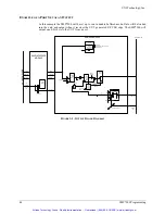
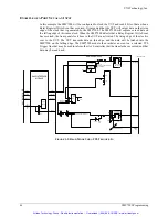
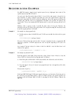
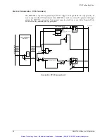
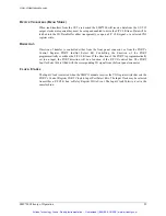
In this example the SMP7500 will be set up to run in double buffered mode. Data will be loaded 
into the unit, and output when it receives the UUT generated F/P CLK edge. The SMP7500 will 
output one 8-bit byte to the UUT from a port. 

USER CONNECTOR

DATA

GND_CLK

GLOBAL

 CLK

Off To All Other Ports

47K

User Selectable 

HW Jumpers

120

100pf

2
2

Output 
Drivers

Over 

Current 
Sense /  
Control

Over Current Sense
 Shut Down

ISENSE

Double 
Buffered

Latched 

Output 

Data 

Buffer

R/B

Control

Writes to 

Specific Port 

Addresses

Control

Control

Relay Req. 000Ch Write Event
WR EVENT

R/B

I/O Data 

Buffer

Data

Control

SMIP INTERFACE 

MODULE

DATA

ADDRESS

CONTROL

BUSYN

TTL 

TRIGGER

BUS

0-7

DATA

ADDRESS

CONTROL

V

X

I  

BAC

KPL

AN

E

SMP7500 MODULE

Over Current 
Reset

Control

Trace 

Memory

Backplane Load


F

IGURE 

3-2:


O

UTPUT 

B

LOCK 

D

IAGRAM


Artisan Technology Group - Quality Instrumentation ... Guaranteed | (888) 88-SOURCE | www.artisantg.com

Содержание SMP7500

Страница 1: ...service in house repair center WE BUY USED EQUIPMENT Sell your excess underutilized and idle used equipment We also offer credit for buy backs and trade ins www artisantg com WeBuyEquipment REMOTE IN...

Страница 2: ...ITAL I O MODULE USER S MANUAL P N 82 0058 000 Released July 31 2009 VXI Technology Inc 2031 Main Street Irvine CA 92614 6509 949 955 1894 Artisan Technology Group Quality Instrumentation Guaranteed 88...

Страница 3: ...VXI Technology Inc 2 Artisan Technology Group Quality Instrumentation Guaranteed 888 88 SOURCE www artisantg com...

Страница 4: ...ecting the Extended Memory Space 19 Front Panel Interface Wiring 20 Hardware Jumper Selection 21 Hardware Resistor Network Pull Up Selection 22 SECTION 3 25 PROGRAMMING 25 Introduction 25 Register Acc...

Страница 5: ...Clock Enable 56 Data Load 56 Device Triggering TTL Trigger 58 Device Transfers Read Mode 59 Direction 59 Clock Enable 59 Latch Data 61 Read Data 61 INDEX 62 Artisan Technology Group Quality Instrumen...

Страница 6: ...VTI from another country VTI warrants that its software and firmware designated by VTI for use with a product will execute its programming when properly installed on that product VTI does not however...

Страница 7: ...CE mark accordingly The product has been designed and manufactured according to the following specifications SAFETY EN61010 2001 EMC EN61326 1997 w A1 98 Class A CISPR 22 1997 Class A VCCI April 2000...

Страница 8: ...he product ATTENTION Important safety instructions Frame or chassis ground Indicates that the product was manufactured after August 13 2005 This mark is placed in accordance with EN 50419 Marking of e...

Страница 9: ...connected to earth ground Operating Conditions To avoid injury electric shock or fire hazard Do not operate in wet or damp conditions Do not operate in an explosive atmosphere Operate or store only in...

Страница 10: ...6 447 8950 Fax 216 447 8951 VTI Instruments Lake Stevens Instrument Division 3216 Wetmore Avenue Suite 1 Everett WA 98201 Phone 949 955 1894 Fax 949 955 3041 VTI Instruments Pvt Ltd Bangalore Instrume...

Страница 11: ...VXI Technology Inc 10 SMP7500 Preface Artisan Technology Group Quality Instrumentation Guaranteed 888 88 SOURCE www artisantg com...

Страница 12: ...VXI module This would allow as many as 576 for a double wide or 192 digital I O for a single wide VXI Module In addition the SMP7500 may be combined with any of the other members of the SMIP family to...

Страница 13: ...rammable polarity through VXI A24 32 registers as an active high or low Input 0 V to 60 V VIN high 2 0 V VIN low 1 5 V input impedance 65 k Output Open collector N DMOS 0 V to 60 V up to 300 mA contin...

Страница 14: ...l register There is also a Global Clock Line from the front panel that may be user selected via hardware jumpers to drive selected PORT clocks By using the appropriate clocking configuration very larg...

Страница 15: ...rs 120 100pf 2 2 Polarity Enable 200K 33K Output Drivers Over Current Sense Control Over Current Sense Shut Down ISENSE Immediate Double Buffered Latched Output Data Buffer Polarity R B Control Writes...

Страница 16: ...d voltage comparator on the input side CHANNEL INPUT CHARACTERISTICS VIN high VIN low VIN max Input Impedance 2 0 V 1 5 V 60 V 65 k CHANNEL OUTPUT CHARACTERISTICS VOUT max Current Sink Maximum Switch...

Страница 17: ...VXI Technology Inc 16 SMP7500 Introduction Artisan Technology Group Quality Instrumentation Guaranteed 888 88 SOURCE www artisantg com...

Страница 18: ...n CALCULATING SYSTEM POWER AND COOLING REQUIREMENTS It is imperative that the chassis provide adequate power and cooling for this module Referring to the chassis operation manual confirm that the powe...

Страница 19: ...25 first convert the decimal number to the hexadecimal value of 19 Next set the back switch to 1 and the front switch to 9 See Figure 2 1 Here are a couple of conversion examples Example 1 LA decimal...

Страница 20: ...Address assignments for individual modules are handled through the A24 A32 address space allocation SELECTING THE EXTENDED MEMORY SPACE The Extended Memory Space of the SMIP II is set by a dip switch...

Страница 21: ...CLK4 10 GND CLK5 11 DATA1 2 11 DATA3 2 11 DATA5 2 11 GND IO4 11 GND IO5 12 DATA1 3 12 DATA3 3 12 DATA5 3 12 GND 12 GND 13 DATA1 4 13 DATA3 4 13 DATA5 4 13 CLAMP6 13 CLAMP7 14 DATA1 5 14 DATA3 5 14 DA...

Страница 22: ...O lines may be overridden either by a hardware jumper setting or programmatically to set the port direction to output If set to GrouND these lines can be used as additional user employable Ground pin...

Страница 23: ...y Inc does not carry other values of these resistor networks Front Panel CLAMP Lines The F P CLAMP lines are available for user defined voltages that are to be used to suppress inductive fly back tran...

Страница 24: ...59 2 to 3 J60 2 to 3 J61 2 to 3 J62 2 to 3 J63 2 to 3 J64 2 to 3 J65 2 to 3 J66 2 to 3 HARDWARE JUMPERS INSTALLED HW HARD WIRED via JUMPER FUNCTION PORT 6 PORT 7 PORT 8 PORT 9 PORT 10 PORT 11 GND_I O...

Страница 25: ...VXI Technology Inc 24 SMP7500 Programming Artisan Technology Group Quality Instrumentation Guaranteed 888 88 SOURCE www artisantg com...

Страница 26: ...rsing thus increasing speed ADDRESSING The VTI switching modules utilize either the A24 or A32 space of the shared memory architecture To read or write to a module register a register address needs to...

Страница 27: ...M Start LOW 28 Trace RAM Start HIGH Trace RAM Start HIGH 26 Module 5 4 Used Address Reserved 24 Module 3 2 Used Address Reserved 22 Module 1 0 Used Address Reserved 20 NVM Access Register NVM Access R...

Страница 28: ...Status Register Read Only D15 A24 A32 Active 1 indicates that A24 A32 memory space access is enabled 0 indicates that A24 A32 memory space access is locked out D14 MODID 1 indicates that the module i...

Страница 29: ...16 D7 D4 Major Hardware Version Number Depends on the specific hardware revision of the SMIP II interface board D3 D0 Minor Hardware Version Number Depends on the specific hardware revision of the SMI...

Страница 30: ...mory Device Always reads as 7FFD16 NVM Access Register Read D15 D1 Unused All Bits are always 1 D0 Reads back the serial data stream from the selected SMIP II board Note that only one SMIP II board ma...

Страница 31: ...D15 D0 Sets the 16 least significant bits of the ending address of the Trace RAM allowing the available RAM to be divided into multiple traces Trace RAM Address HIGH Register Read and Write D15 D4 Un...

Страница 32: ...etting a bit to a 1 enables the trigger line setting a bit to 0 disables the corresponding line All bits are set to 0s when either a soft or a hard reset is received by the module D7 D0 Sets the TTLTR...

Страница 33: ...ion sent by the plug in modules D15 corresponds to TTLTRIG7 D14 to TTLTRIG6 and D8 to TTLTRIG0 Setting a bit to a 1 enables the trigger line setting a bit to a 0 disables the corresponding line All bi...

Страница 34: ...he relays on module 3 have settled a 1 indicates that the relays on module 3 are still changing state D2 A 0 read from this bit indicates the relays on module 2 have settled a 1 indicates that the rel...

Страница 35: ...s Relay Space Utilized as shown in the Relay Register Map See Module Appendices Unused Module 5 Configuration 512 bytes Module 4 Configuration 512 bytes Module 3 Configuration 512 bytes Module 2 Confi...

Страница 36: ...ister 228 Control Reg Relay Register Write Event Select 226 Control Reg BUSYN Delay Timer 224 Control Reg BUSYN Select 222 Control Reg F P CLK Select 220 Control Reg F P CLK Lines R B 21E Control Reg...

Страница 37: ...te hFF PORT 7 6 Read and Write D7 D0 PORT 6 Digital I O PORT 6 Pon state hFF D15 D8 PORT 7 Digital I O PORT 7 Pon state hFF PORT 9 8 Read and Write D7 D0 PORT 8 Digital I O PORT 8 Pon state hFF D15 D8...

Страница 38: ...0 respectively 1 Relay Register Write Event MUX 2 Relay Register 000Ch Write Event 3 F P CLK Select MUX Pon state 0 D5 PORT Clock to PORT Output Polarity Select Set to 0 for non inverted Port Clock o...

Страница 39: ...REGISTER F P OVER CURRENT SENSE Read D15 D0 Over Current Sense Lines 15 0 Read Back The SMP7500 has 16 separate over current sense circuits This is due to the nature of the output drivers that are use...

Страница 40: ...is dependent on the setup of the F P In Outn lines 11 thru 6 If the F P lines are used as GND then the read back lines are pulled to a logic 1 If the F P lines are used as inputs or outputs then a re...

Страница 41: ...CLK and then on to the proper PORT CLK as desired Pon state 0 D7 D3 Unused These bits are unused D10 D8 F P CLK Select for PORTs 11 thru 6 Value Clock selected 0 GND 1 F P CLK 6 2 F P CLK 7 3 F P CLK...

Страница 42: ...ely note that if a Port F P CLK other than 6 thru 11 is desired to be used as the source for the BUSYN signal then the BUSYN Select Bits for F P CLKs 0 thru 5 should be utilized to connect the desired...

Страница 43: ...CONTROL REGISTER BUSYN DELAY TIMER Read and Write D15 D0 BUSYN Delay Timer When using the BUSYN Delay Timer this register is used to set the time that the plug in module will time before producing a B...

Страница 44: ...LED on Pon state 0 D9 Relay Reset Select Bit Set to 0 so that the Openbus signal is not selected to reset this module s Ports Set to 1 to select the Openbus signal to reset this module s Ports Pon st...

Страница 45: ...table HW Jumpers 120 100pf 2 2 Output Drivers Over Current Sense Control Over Current Sense Shut Down ISENSE Double Buffered Latched Output Data Buffer R B Control Writes to Specific Port Addresses Co...

Страница 46: ...set to 0 to allow the external F P CLK input as the trigger method to output data to the UUT By setting the PORT Clock to Port Output Polarity Bit either positive or negative edge operation of the cl...

Страница 47: ...falling edge The SMP7500 module then initiates an event on a selected TTL Trigger line that may be used to inform the slot 0 controller that the transfer has occurred and that data may be read back US...

Страница 48: ...ORT Output Clock Select Bits are set to 2 to select the Relay Register write Event The PORT Output Clock Polarity Select Bit should then be set for positive edge sensitivity This bit is set to 0 in th...

Страница 49: ...SENSE R B Control Writes to Specific Port Addresses Control Control Relay Req 000Ch Write Event WR EVENT R B I O Data Buffer Data Relay Req 000Ch Write Event SMIP INTERFACE MODULE DATA ADDRESS CONTROL...

Страница 50: ...Setup PORT 2 Set PORT 2 s PORT Inn Out Select Bit to 0 set PORT 2 as an input port PORT 2 Control Register h0000 Set PORT 2 s PORT Clock to Input Port Select Bits to 0 selects the F P CLK 2 Set PORT 2...

Страница 51: ...e Relay Register Write Event is initiated the F P CLK output signal from PORT 0 is transmitted to the F P CLK input signal of PORT 2 The data on PORT 0 s outputs are now clocked into PORT 2 The data w...

Страница 52: ...iven below 1111000010101010 in binary format The lower 8 bits are the current value for Port 1 In order to maintain its value an appropriate OR operation is required A bit shift operation may also be...

Страница 53: ...VXI Technology Inc 52 SMP7500 Programming Artisan Technology Group Quality Instrumentation Guaranteed 888 88 SOURCE www artisantg com...

Страница 54: ...o a clock source Transparent Mode This refers to the method of operation of a PORT For example if the PORT is being used as an output then as soon as the data is written it will appear on the external...

Страница 55: ...VXI Technology Inc 54 SMP7500 Command Dictionary Artisan Technology Group Quality Instrumentation Guaranteed 888 88 SOURCE www artisantg com...

Страница 56: ...llel data words to be transmitted or received The SMP7500 contains the capability to generate a TTL trigger onto the VXI backplane using either a VXI register write or F P CLK event By utilizing the D...

Страница 57: ...he direction of the PORT is programmatically set to an output the PORT will be an output The PORT Inn Out Select Bit is OR ed with the corresponding I O signal from the front panel connector CLOCK ENA...

Страница 58: ...d Output Data Buffer R B Control Writes to Specific Port Addresses Control Control Relay Req 000Ch Write Event WR EVENT R B I O Data Buffer Data Control SMIP INTERFACE MODULE DATA ADDRESS CONTROL BUSY...

Страница 59: ...Left Floating DATA GND_CLK GLOBAL CLK 47k User Selectable HW Jumpers 22 Off To All Other Ports 47K User Selectable HW Jumpers 120 100pf 2 2 Enable set 200K 33K R B Control Writes to Specific Port Add...

Страница 60: ...it Controlling the direction of the PORT programmatically overrides the F P CLK lines If the direction of the PORT is programmatically set to an input the PORT direction will be a function of the F P...

Страница 61: ...pecific Port Addresses Control Control Relay Req 000Ch Write Event WR EVENT R B I O Data Buffer Data Backplane Load Transparent Relay Req 000Ch Write Event Control SMIP INTERFACE MODULE DATA ADDRESS C...

Страница 62: ...load the UUT driving source LATCH DATA The selected edge of the selected Input Clock signal event then clocks the I O Data Buffer to read data from the UUT The selected Input Clock signal may also be...

Страница 63: ...56 59 Device triggering 58 Digital I O Module 17 35 51 drivers 38 dynamic configuration 27 E Event MUX 37 38 40 41 42 Extended Memory 19 29 35 Extended Memory Device 29 Extended Memory Space 19 exter...

Страница 64: ...32 38 39 43 Reset 27 resistor network 22 resistor networks 22 S SCPI 55 Select MUX 37 38 40 sense circuits 38 Serial clock 29 Serial data 29 shroud 20 signal bounce 21 Switch on time 15 switching tran...

Страница 65: ...service in house repair center WE BUY USED EQUIPMENT Sell your excess underutilized and idle used equipment We also offer credit for buy backs and trade ins www artisantg com WeBuyEquipment REMOTE IN...

Отзывы: