TOSHIBA
TMPR3904F Rev. 2.0
141
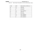
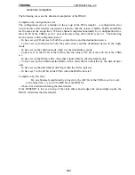
26
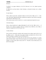
Edge Mode
In the edge mode, the internal DREQn signal (dreq) is edge-detected. If the valid edge of the
dreq signal is acknowledged at a rising of the internal clock (GCLK) (if it is presently at the
active level although it was not at the active level at the rising of one GCLK before) when the
channel is in the wait status, the DMAC acknowledges that there is a transfer request and
switches to the transfer status to start the transfer operation. The active edge (falling or rising)
of the DREQn signal is set up in the PosE bit of the CCRn. The active level of the DACKn
signal is at high when a rising of the DREQn signal is on the valid edge, and at low when a
falling of the DREQn signal is on the active edge.
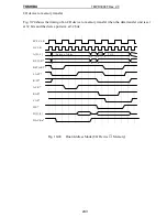
If the valid edge of the dreq signal is acknowledged by a rising of the GCLK that acknowledges
the assertion of the acknowledge signal (which is generated by the on-chip memory controllers
at a memory access in the dual address mode or in the single address mode, or is the same as the
ACK* singal at an I/O access in the dual address mode), the next data transfer is conducted
immediately afterwards. However, if a transfer request is generated on another channel with a
higher priority, a channel transit takes place.
If there is no valid edge of the dreq signal by the rising of the GCLK that acknowledges the
assertion of the acknowledge signal, it is understood that there is no transfer request so that a
transfer operation on another channel may be started or the bus ownership may be released to be
in the wait status.
The acknowledge signal is recognized at the rising edge of the GCLK which precedes the
GCLK cycle when the final LAST* signal for a data transfer is negated.
The unit of the transfer request is designated in the TrSiz field of the CCRn.
S Y S C L K
d r e q
D R E Q n
( B u s o w n e r s h i p r e q u e s t )
A c k n o w l e d g e s i g n a l
( B u s o w n e r s h i p
r e l e a s e n o t i c e )
A [ 3 1 : 1 ]
• A
B E [3:0]*
R / W *
B S T A R T *
D A C K n
D a t a t r a n s f e r
D a t a t r a n s f e r
T h e d r e q , t h e b u s o w n e r s h i p r e q u e s t s i g n a l , t h e b u s o w n e r s h i p r e l e a s e n o t i c e s i g n a l a n d t h e a c k n o w l e d g e
s i g n a l a r e i n t e r n a l s i g n a l s o f t h e T X 3 9 0 4 .
Fig. 10-19 Transfer Request Timing (Edge Mode)
Содержание TMPR3904F
Страница 1: ...Users Manual 32bit RISC Microprocessor TX39 family TMPR3904F Rev 2 0 Jan 12 1998 ...
Страница 2: ......
Страница 9: ...Users Manual 01 1 INTRODUCTION 1 1 Overview ...
Страница 10: ...Users Manual 02 1 2 Notation used in this manual Mathematical notation Data notation Signal notation ...
Страница 11: ...Users Manual 03 1 3 Kind of accessing by the TX3904 ...
Страница 12: ...Users Manual 04 1 4 Precautions in the TMPR3904F specification Don t set Don t use ...
Страница 13: ...Users Manual 05 Do not use ...
Страница 14: ...Users Manual 06 ...
Страница 15: ...Users Manual 7 2 FEATURES n n n n n n n n n n n n n ...
Страница 16: ...Users Manual 8 ...
Страница 18: ...Users Manual 10 ...
Страница 19: ...Users Manual 11 4 PINS 4 1 Positions of Pins ...
Страница 20: ...Users Manual 12 ...
Страница 21: ...Users Manual 13 4 2 Functions of Pins ...
Страница 22: ...Users Manual 14 ...
Страница 23: ...Users Manual 15 ...
Страница 24: ...Users Manual 16 ...
Страница 26: ...Users Manual 18 5 2 Register Map ...
Страница 27: ...Users Manual 19 ...
Страница 28: ...Users Manual 20 ...
Страница 30: ...Users Manual 22 5 3 2 PIO2 and PIO1 ...
Страница 32: ...Users Manual 24 5 3 4 Connection of external bus master 5 3 5 INT 7 0 active status clear ...
Страница 33: ...Users Manual 25 5 3 6 INT 7 0 active status set up ...
Страница 34: ...Users Manual 26 ...
Страница 123: ...TOSHIBA TMPR3904F Rev 2 0 115 26 ...
Страница 169: ...TOSHIBA TMPR3904F Rev 2 0 161 26 ...
Страница 203: ...TOSHIBA TMPR3904F Rev 2 0 195 ...
Страница 230: ......

