background image

TOSHIBA 


TMPR3904F Rev. 2.0


94

 9.4

Operations

9.4.1

Channel select

The channel select for memory access is conducted by the address that is given onto the GBUS
of the internal system bus.
Of the addresses, the high-order 12 bits are compared if they are within the range from the base
address that is set up in the channel control register to the size that is set up in the size register,
and if they are in the range, the channel is selected.  The base address can be masked.  Masking
is conducted by the base address mask register that designates at will a mask with 12-bit base
address.

Table 9-2     Address Decode

Ch. Size

Bank Size

Ch. Select

Base Addr. bit

Bank 1

Bank 0

Bank 1

Bank 0

1M

512K

A31:20

A19=1

A19=0

A19=1

A19=0

2M

1M

A31:21

A20=1

A20=0

A20=1

A20=0

4M

2M

A31:22

A21=1

A21=0

A21=1

A21=0

8M

4M

A31:23

A22=0

A22=1

A22=1

A22=0

16M

8M

A31:24

A23=0

A23=1

A23=1

A23=0

32M

16M

A31:25

A24=0

A24=1

A24=1

A24=0

Size

A31

A30

A29

A28

A27

A26

A25

A24

A23

A22

A21

A20

A19

1M

*

*

*

*

*

*

*

*

*

*

*

*

#

2M

*

*

*

*

*

*

*

*

*

*

*

#

4M

*

*

*

*

*

*

*

*

*

*

#

8M

*

*

*

*

*

*

*

*

*

#

16M

*

*

*

*

*

*

*

*

#

32M

*

*

*

*

*

*

*

#

*:  The bit to be compared with the base address to select the channel
#:  To be used to select the bank

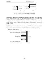
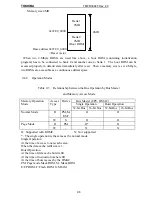
Depending on the set-up of the base address and the size of each channel, two channels are
sometimes selected.  In such a case, the channel to which a higher base address is set up is
selected.  When accessing the addresses shown in Figure 9-9, Channel 1 with a higher base
address value is selected.  When the same base address is set up, Channel 0 has the priority to be
selected.

Bank Sel.(Ch0)

Bank Sel.(Ch1)

Содержание TMPR3904F

Страница 1: ...Users Manual 32bit RISC Microprocessor TX39 family TMPR3904F Rev 2 0 Jan 12 1998 ...

Страница 2: ......

Страница 3: ...2 5 3 3 Error processing 23 5 3 4 Connection of external bus master 24 5 3 5 INT 7 0 active status clear 24 5 3 6 INT 7 0 active status set up 25 6 CLOCK 26 6 1 Clock Generator 27 6 2 Operation Modes of TX3904 27 6 2 1 Normal mode 27 6 2 2 Halt mode 27 6 2 3 Doze mode 28 6 2 4 RF Reduced Frequency mode 28 6 3 Status Shifting 29 6 4 Operations of each block in the each modes 30 7 BUS OPERATIONS 31 ...

Страница 4: ...8 4 1 Channel control register 0 DCCR0 54 8 4 2 Base address mask register 0 DBMR0 56 8 4 3 Wait register 0 DWR0 57 8 4 4 Channel control register 1 DCCR1 59 8 4 5 Base address mask register 1 DBMR1 61 8 4 6 Wait register 1 DWR1 62 8 4 7 Refresh control register DREFC 64 8 5 Operations 65 8 5 1 Channel select 65 8 5 2 Address multiplex 66 8 5 3 Operation modes 67 8 5 4 32 16 bit static bus sizing ...

Страница 5: ... CONTROLLER ROMC 85 9 1 Features 85 9 2 Block Diagrams 86 9 3 Registers 87 9 3 1 Channel control register 0 88 9 3 2 Channel control register 1 90 9 3 3 Base address mask register 0 92 9 3 4 Base address mask register 1 93 9 4 Operations 94 9 4 1 Channel select 94 9 4 2 Operation Modes 96 9 4 3 32 16 bit Static Bus Sizing 97 9 4 4 16 bit Bus Access 97 9 4 5 Access by External Bus Master 97 9 4 6 P...

Страница 6: ...internal blocks 118 10 2 3 Priority between modules 118 10 3 Registers 120 10 3 1 DMA control register DCR 121 10 3 2 Channel control register CCRn 122 10 3 3 Channel status register CSRn 126 10 3 4 Source address register SARn 129 10 3 5 Destination address register DARn 130 10 3 6 Byte count register BCR0n 131 10 3 7 Next byte count register NCR0 1 132 10 3 8 Data holding register DHR 133 10 4 F...

Страница 7: ...Rn 173 12 3 2 Line status register SLSRn 175 12 3 3 DMA Interrupt control register SDICRn 176 12 3 4 DMA Interrupt status register SDISRn 178 12 3 5 FIFO control register SFCRn 180 12 3 6 Baudrate control register SBGRn 181 12 3 7 Transmit FIFO buffer TFIFOn 182 12 3 8 Receive FIFO buffer SFIFOn 182 12 4 Operations 183 12 4 1 Overview 183 12 4 2 Data format 183 12 4 3 Serial clock generator 185 12...

Страница 8: ... TCR2 1 0 200 13 3 2 Interval timer mode registers 0 1 and 2 ITMR2 1 0 202 13 3 3 Divider registers 2 1 and 0 CCDR2 1 0 203 13 3 4 Pulse generator mode registers 2 and 1 PGMR2 1 204 13 3 5 Watchdog timer mode register 2 WTMR2 205 13 3 6 Timer interrupt status registers 2 1 and 0 TISR2 1 0 206 13 3 7 Compare registers A 2 1 and 0 CPRA2 1 0 208 13 3 8 Compare registers B 2 1 and 0 CPRB2 1 0 208 13 3...

Страница 9: ...Users Manual 01 1 INTRODUCTION 1 1 Overview ...

Страница 10: ...Users Manual 02 1 2 Notation used in this manual Mathematical notation Data notation Signal notation ...

Страница 11: ...Users Manual 03 1 3 Kind of accessing by the TX3904 ...

Страница 12: ...Users Manual 04 1 4 Precautions in the TMPR3904F specification Don t set Don t use ...

Страница 13: ...Users Manual 05 Do not use ...

Страница 14: ...Users Manual 06 ...

Страница 15: ...Users Manual 7 2 FEATURES n n n n n n n n n n n n n ...

Страница 16: ...Users Manual 8 ...

Страница 17: ...UT A 31 24 PIO2 7 0 B E 3 0 D 31 0 R W BSTART HAVEIT PIO1 2 ACK B U S E R R B U S R E L PIO1 3 B U S R E Q PIO1 1 B U S G N T PIO1 0 SYSCLK TMR0 N M I TEST2 HALF SCS 3 0 T E S T C L K E N P L L O F F Debug Interface S I N 0 S O U T 0 CTS0 S I N 1 S O U T 1 CTS1 RAS1 0 3 0 CAS 3 0 W E O E 1 0 CE1 0 1 0 S W E 1 0 S C L K I N TMR1 TMR2 T I M O U T 1 T I M O U T 2 T I M I N 2 T I M I N 1 D O N E R E S...

Страница 18: ...Users Manual 10 ...

Страница 19: ...Users Manual 11 4 PINS 4 1 Positions of Pins ...

Страница 20: ...Users Manual 12 ...

Страница 21: ...Users Manual 13 4 2 Functions of Pins ...

Страница 22: ...Users Manual 14 ...

Страница 23: ...Users Manual 15 ...

Страница 24: ...Users Manual 16 ...

Страница 25: ...rtual Address Physical Address Cache Mode kseg2 Reserved Area 0xFFFF_FFFF 0xFF00_0000 0xFFFF_FFFF 0xFF00_0000 Impossible Kernel kseg2 0xFEFF_FFFF 0xC000_0000 0xFEFF_FFFF 0xC000_0000 Possible Kernel kseg1 0xBFFF_FFFF 0xA000_0000 0x1FFF_FFFF 0x0000_0000 Impossible Kernel kseg0 0x9FFF_FFFF 0x8000_0000 0x1FFF_FFFF 0x0000_0000 Possible Kernel kuseg 0x7FFF_FFFF 0x7F0000_000 0 0xBFFF_FFFF 0xBF00_0000 Imp...

Страница 26: ...Users Manual 18 5 2 Register Map ...

Страница 27: ...Users Manual 19 ...

Страница 28: ...Users Manual 20 ...

Страница 29: ...1 21 30 29 28 27 26 25 24 23 20 16 15 1 0 Type Initial Value Type Initial Value 0 EIClr POBus S1D S0D P2En P1En TOE WR R W R W R W R W R W R W R W W R W R W R W R W R W R W R W R W 0 00 0 0 0 0 0 00 00 00 00 00 00 00 00 2 12 13 14 11 10 9 5 6 8 7 4 3 BEOW 17 0 R W 5 3 1 DMA transfer of SIO ...

Страница 30: ...Users Manual 22 5 3 2 PIO2 and PIO1 ...

Страница 31: ...erated by a write operation of the TX39 processor core Notification of anomaly is sent due to a non maskable interrupt if one of the following occurs access of nonexistent register access of nonexistent address 0xFFFF_Dxxx or BUSERR signal assert Simultaneous to this sets the BEOW bit to 1 and indicates that a bus error was the cause of the non maskable interrupt 1 Non maskable interrupt was gener...

Страница 32: ...Users Manual 24 5 3 4 Connection of external bus master 5 3 5 INT 7 0 active status clear ...

Страница 33: ...Users Manual 25 5 3 6 INT 7 0 active status set up ...

Страница 34: ...Users Manual 26 ...

Страница 35: ...operations by halting the clocks inside the TX39 Processor Core By setting the halt bit of the Config register of the TX39 Processor Core it shifts to the halt mode When having entered into the halt mode the TX39 mega cell core halts the operation while maintaining the pipeline status Bus release requests from GREQ and HPGREQ can be replied to but those from the SREQ and HPSREQ are not replied to ...

Страница 36: ...red into the doze mode the TX39 mega cell core halts operations while maintaining the pipeline status The write buffer does not halt Therefore if there are remaining data in the write buffer in the doze mode the write operation continues until the buffer becomes empty The SYSCLK does not halt either The doze mode is recovered from when the doze bit is cleared to 0 by asserting the interrupts by on...

Страница 37: ...ield for the peripheral macro cell s and the mega cell core in the parts that are not affected by frequency changes 6 3 Status Shifting The following diagram shows shifts of the modes Normal Mode Halt Mode RF Mode Config Halt 1 Config RF 1 0 NEQ 00 Config RF 1 0 00 Interupt RF 00 Config Halt 1 Interupt RF NEQ 00 RF NEQ 00 Doze Mode Config Doze 1 Interupt RF 00 Config Doze 1 Interupt RF NEQ 00 Fig ...

Страница 38: ... Halts DRAMC Refresh function Operation Operation 1 No change Others Halts Change ROMC All functions Operation Halts Change DMAC All functions Operation Halts Change IRC All functions Operation Operation Change SIO For transmitter receiver clock generation Operation Operation No change Others Change TMR Counter operation Operation Operation No change Others Change PIO All functions Operation Halts...

Страница 39: ...nd the single write operation 7 1 1 System chip select In the TX3904 there are four system chip select signals SCS 3 0 These signals are a low active select signal made by decoding the high order bit of the address that the TX39 Processor Core or the built in DMAC outputs The SCS 3 0 is set up in three registers of the EBIF Table 7 1 Register Map for System Chip Select Address Module Register 0xFF...

Страница 40: ...tion 31 24 CS3Addr SCS3 address SCS3 Address initial value 0x20 Asserts a CS3 signal when the high order 8 bits A 31 24 of the address physical address matches the CS3Addr The efficient range of the CS3Addr shall be set up in the CS3Mask field of the SCS Mask register 23 16 CS2Addr SCS2 address SCS2 Address 15 8 CS1Addr SCS1 address SCS1 Address 7 0 CS0Addr SCS0 address SCS0 Address Fig 7 1 SCS Ad...

Страница 41: ...escription 31 2 4 CS3Mas k SCS3 mask SCS3 Mask initial value 0xFF Specifies the valid bit of the address comparison by the CS3Addr field of the SCS Address register 1 Bit of the corresponding CS3Addr field is compared 0 Bit of the corresponding CS3Addr field is not compared 23 1 6 CS2Mas k SCS2 mask SCS2 Mask 15 8 CS1Mas k SCS1 mask SCS1 Mask 7 0 CS0Mas k SCS0 mask SCS0 Mask Fig 7 2 SCS Mask Regis...

Страница 42: ...f the area SCS 3 is 32 bits 1 The data width of the area SCS 3 is 16 bits 26 2 4 CS3Wait CS3 wait CS3 Wait Sets up the number of waits for the SCS 3 signal Executes the bus operation with the set up number of waits If it is set up to 111 drive the ACK signal from outside 000 0 Wait 001 1 Wait 010 2 Waits 011 3 Waits 100 4 Waits 101 5 Waits 110 6 Waits 111 External ACK Input 19 CS216 CS2 16 bits CS...

Страница 43: ...T 1 T 2 T 3 T 4 T1 Outputs the value s valid to A 31 1 and BE 3 0 At the same time asserts BSTART and LAST Asserts SCS 3 0 also if the address is in the SCSn area The R W becomes high because it is a read operation T2 Deasserts the BSTART T3 Deasserts the LAST because it has acknowledged that the ACK is low When a wait is designated in the SCS wait register the input of the ACK signal is not neces...

Страница 44: ...t the same time asserts BSTART and LAST Asserts SCS 3 0 also if the address is in the SCSn area The R W becomes high because it is a read operation T2 Deasserts the BSTART T3 Becomes the wait cycle because the ACK is high T4 Deasserts the LAST because it has acknowledged that the ACK is low When a wait is designated in the SCS wait register the input of the ACK signal is not necessary Please input...

Страница 45: ... the value valid to A 31 1 The BE 3 0 is always low Asserts BSTART Does not assert LAST This point that it does not assert the LAST is the difference from the single read operation Asserts the SCS 3 0 when the address is in the SCSn area The R W becomes high because it is a read operation T2 Deasserts the BSTART T3 Reads in data at the timing of T3 because the ACK is low T4 Reads in the first datu...

Страница 46: ...ACK signal The following diagram shows the operation in the case where a wait cycle is entered while the first and third data are being read If SCS is used the number of waits cannot be changed at each datum R W ACK B U S E R R D 31 0 S C S 3 0 SYSCLK A 31 1 B E 3 0 BSTART LAST T1 T2 T3 T4 T5 T6 T7 T8 T9 w a i t w a i t ...

Страница 47: ...4 T1 Outputs the value s valid to A 31 1 and BE 3 0 At the same time asserts BSTART and LAST Asserts SCS 3 0 also if the address is in the SCSn area The R W becomes low because it is a write operation Outputs the value valid to D 31 0 T2 Deasserts the BSTART T3 Deasserts the LAST because it has acknowledged that the ACK is low When a wait is designated in the SCS wait register the input of the ACK...

Страница 48: ... At the same time asserts BSTART and LAST Asserts SCS 3 0 also if the address is in the SCSn area The R W becomes low because it is a write operation Outputs the value valid to D 31 0 T2 Deasserts the BSTART T3 Becomes the wait cycle because the ACK is high T4 Deasserts the LAST because it has acknowledged that the ACK is low When a wait is designated in the SCS wait register the input of the ACK ...

Страница 49: ...egister area inside the TX3904 Also a bus error is generated when the external bus master attempts to access the inside of the TX3904 0xFFxx_xxxx A bus error exception is generated during read operation by the TX39 processor core A nonmaskable interrupt exception is generated during a write operation by the TX39 processor core 7 2 3 Time out error If there is no response within 256 SYSCLK after th...

Страница 50: ...e TX3904 on chip DMA controller The DMA controller immediately suspends transfer operation then abnormally ends the channel operation During bus operation of the external bus master The TX3904 asserts BUSERR signal SYSCLK BSTART ACK Bus Error 1 2 3 255 256 ...

Страница 51: ...f the EBIF as for the area of the SCSn In the 16 bit bus mode a 32 bit operation of the TX39 Processor Core shall be executed in two 16 bit bus operations The following diagram shows the relationship between the memory and the data bus register 15 0 A B C 04 02 00 M e m or y I m a g e A B 31 0 Register Data Bus Image If the data to be handled can fit in the upper or lower half word during a 16 bit...

Страница 52: ... 44 As an example the following diagram shows the word access in the case where the SCSn area is 16 bit bus one wait SYSCLK A 31 1 B E 3 0 BSTART LAST R W A 1 0 A 1 1 H H L L H H L L ACK BUSERR D 15 0 S C S 3 0 D1 D2 wait wait ...

Страница 53: ...s connected to the TX3904 the TX39 Processor Core operates at 50 MHz and usually the full speed bus mode the bus operation is also at 50 MHz In the half speed bus mode the bus operation becomes 25 MHz The frequency of the SYSCLK also changes It is to be set up with the HALF signal whether to make it operate in the half speed bus mode or not When the HALF signal is low it is the half speed bus mode...

Страница 54: ...rts the BUSGNT signal When the external bus master has acquired the bus ownership it has to assert the HAVEIT signal The BUSREQ and HAVEIT signals must be asserted until releasing the bus ownership The following diagram shows the timing of the bus ownership being granted to an external bus master SYSCLK B U S R E Q B U S G N T HAVEIT B U S R E L T1 T2 T3 T4 T5 TX3904 Cycle Dead Cycle E x t e r n a...

Страница 55: ... external bus master deasserts the BUSREQ and HAVEIT to return the bus ownership to the TX3904 The following diagram shows the timing of releasing the bus ownership when it is no longer necessary SYSCLK B U S R E Q B U S G N T HAVEIT B U S R E L T1 T2 T3 T4 T5 TX3904 Cycle Dead Cycle E x t e r n a l B u s Master Cycle T1 The external bus master has the bus ownership T2 The external bus master deas...

Страница 56: ...ease of the bus ownership by BUSREL BUSREQ does not have to be de asserted Also the release request of the bus ownership may be left unanswered The following diagram shows the timing of the bus ownership release by BUSREL SYSCLK B U S R E Q B U S G N T HAVEIT B U S R E L T1 T2 T3 T4 T5 TX3904 Cycle Dead Cycle E x t e r n a l B u s Master Cycle T1 The TX3904 asserts BUSREL T2 The external bus maste...

Страница 57: ...Q the snoop function of the TX39 Processor Core works With HPGREQ and GREQ the snoop function does not work The snoop function is explained in the next section 7 5 4 Snoop function The TX39 Processor Core has a snoop function It is a function to maintain consistency between the data cache of the TX39 Processor Core and the data of an external memory When the snoop function of the TX39 Processor Co...

Страница 58: ...e status of the INT 7 0 is set up at the low level or the high level the interrupt request must be cleared at the origin of the interrupt request When the active status is set up at the rising edge or the falling edge clear the interrupt request in the EIClr field of the CConR 7 6 2 NMI The NMI is a non maskable interrupt request signal This interrupt cannot be masked When the NMI is asserted the ...

Страница 59: ...its The number of penalty cycles at the page hit miss 3 Independent size set up is possible for each channel 1 2 4 8 16 32 64MB The size of the bank must be a quarter of the channel size 4 Support of 32 16 bit static bus sizing The static bus sizing to 32 16 bit bus is possible The bus width of the DRAM is designated at the register set up after reset 5 The fast page mode is supported 6 The hyper ...

Страница 60: ...TSCH SIGNAL FROM EBIF EBIF G BUS G BUS I F SIGNAL MA16 1 Fig 8 1 DRAMC Connection Inside TX3904 Refresh timer CH0 Timing Control HOST I F Address Decorder Ch Reg Address Decorder Ch Reg RAS1 3 0 CAS 3 0 MA 11 0 WE Address MUX CH1 Arbitor Address Control Normal R W FastPage R W EDO R W CBR Refresh CBRS Refresh COL Counter ROW Counter RESET Address Data Control Mask Reg Mask Reg RAS0 3 0 Reg Address...

Страница 61: ...Name 0xFFFF_8000 DCCR0 Channel Control Register 0 0x FFFF_8004 DBMR0 Base Address Mask Register 0 0x FFFF_8008 DWR0 Wait Register 0 0x FFFF_8100 DCCR1 Channel Control Register 1 0x FFFF_8104 DBMR1 Base Address Mask Register 1 0x FFFF_8108 DWR1 Wait Register 1 0x FFFF_8800 DREFC Refresh Control Register ...

Страница 62: ...ss on Channel 0 Designates the row direction size of the DRAM to be connected to each bank on Channel 0 000 512 rows 011 4096 rows 001 1024 rows 1 Reserved 010 2048 rows 14 12 DCW0 DRAM channel 0 column address size DRAM Control Column Word on Channel 0 Designates the column direction size of the DRAM to be connected to each bank on Channel 0 000 128 words 10 2048 words 001 256 words 11 Reserved 0...

Страница 63: ...ved 011 8 Mbytes 2 16BUS0 DRAM channel 0 bus size DRAM Control 16 bit Width Bus Size on Channel 0 Designates the bus width of the memory to be connected to Channel 0 1 16 bit width bus size 0 32 bit width bus size 1 DIM0 Reserved This bit is reserved Do not set to 1 0 DPM0 DRAM channel 0 page mode select DRAM Control Page Mode on Channel 0 Designates the page mode of the DRAM connected to Channel ...

Страница 64: ... of Field Description 31 20 DBAM0 DRAM channel 0 base address mask DRAM Control Base Address Mask on Channel 0 Specifies the valid bit of the address comparison by the DBA0 field of the channel control register 1 Bit of the corresponding DBA0 field is not compared 0 Bit of the corresponding DBA0 field is compared Fig 8 5 DRAM Channel 0 Base Address Mask Register ...

Страница 65: ... 101 5 waits 010 2 waits 110 6 waits 011 3 waits 111 7 waits 18 16 WTE0 DRAM channel 0 external bus master normal mode wait Normal Mode Wait Cycle for External Bus Master Designates the number of wait cycles with which the external bus master accesses the Channel 0 DRAM in the normal mode single mode 000 0 wait 100 4 waits 001 1 wait 101 5 waits 010 2 waits 110 6 waits 011 3 waits 111 7 waits 14 1...

Страница 66: ...aits 111 7 waits 5 4 PWTC0 DRAM channel 0 CPU page mode wait Page Mode Wait Cycle for CPU Designates the number of wait cycles with which the CPU accesses the Channel 0 DRAM in the page mode burst mode 00 0 wait 10 2 waits 01 1 wait 11 3 waits 2 0 WTC0 DRAM channel 0 CPU normal mode wait Normal Mode Wait Cycle for CPU Designates the number of wait cycles with which the CPU accesses the Channel 0 D...

Страница 67: ... Designates the row direction size of the DRAM to be connected to each bank on Channel 1 000 512 rows 011 4096 rows 001 1024 rows 1 Reserved 010 2048 rows 14 12 DCW1 DRAM channel 1 column address size DRAM Control Column Word on Channel 1 Designates the column direction size of the DRAM to be connected to each bank on Channel 1 000 128 words 10 2048 words 001 256 words 11 Reserved 010 512 words 01...

Страница 68: ...ved 011 8 Mbytes 2 16BUS1 DRAM channel 1 bus size DRAM Control 16 bit Width Bus Size on Channel 1 Designates the bus width of the memory to be connected to Channel 1 1 16 bit width bus size 0 32 bit width bus size 1 DIM1 Reserved This bit is reserved Do not set to 1 0 DPM1 DRAM channel 1 page mode select DRAM Control Page Mode on Channel 1 Designates the page mode of the DRAM connected to Channel ...

Страница 69: ...of Field Description 31 20 DBAM1 DRAM channel 1 base address mask DRAM Control Base Address Mask on Channel 1 Specifies the valid bit of the address comparison by the DBA1 field of the channel control register 1 Bit of the corresponding DBA1 field is not compared 0 Bit of the corresponding DBA1 field is compared Fig 8 10 DRAM Channel 1 Base Address Mask Register ...

Страница 70: ...101 5 waits 010 2 waits 110 6 waits 011 3 waits 111 7 waits 18 16 WTE1 DRAM channel 1 external bus master normal mode wait Normal Mode Wait Cycle for External Bus Master Designates the number of wait cycles with which the external bus master accesses the Channel 1 DRAM in the normal mode single mode 000 0 wait 100 4 waits 001 1 wait 101 5 waits 010 2 waits 110 6 waits 011 3 waits 111 7 waits 14 12...

Страница 71: ...its 111 7 waits 5 4 PWTC1 DRAM channel 1 CPU page mode wait Page Mode Wait Cycle for CPU Designates the number of wait cycles with which the CPU accesses the Channel 1 DRAM in the page mode burst mode 00 0 wait 10 2 waits 01 1 wait 11 3 waits 2 0 WTC1 DRAM channel 1 CPU normal mode wait Normal Mode Wait Cycle for CPU Designates the number of wait cycles with which the CPU accesses the Channel 1 DR...

Страница 72: ...Self Refresh Enable Designates whether or not to use the DRAM self refresh function in the halt mode CBRSE Function 0 Disable self refresh 1 Enable self refresh 9 0 DRCYC Refresh cycle DRAM Control Refresh Cycle Specifies the refresh cycle Default is 1100000000 2 It s 15 36 µsec when the internal system clock is 50 MHz 20 nsec per cycle Specify the clock count of the internal system clock in binar...

Страница 73: ...tes at will a mask with 12 bit base address The DRAMC selects the channel and bank according to the following table Table 8 2 Address Decode Ch Size Ban k Size Ch Select Base Addr bit Bank3 Bank2 Bank1 Bank0 1M 256K A31 20 A19 18 11 A19 18 10 A19 18 01 A19 18 00 2M 512K A31 21 A20 19 11 A20 19 10 A20 19 01 A20 19 00 4M 1M A31 22 A21 20 11 A21 20 10 A21 20 01 A21 20 00 8M 2M A31 23 A22 21 11 A22 21...

Страница 74: ...elect 8 5 2 Address multiplex The multiplex of the address allocates the upper addresses to the row address and the lower addresses to the column address to make page mode access effective The number of the column address bits is determined by the DCWn n 0 1 of the DCCRn When the bus width of the DRAM is 16 bits A m 1 m 11 10 9 8 7 becomes the column address and the high order bit that starts from...

Страница 75: ...R W W FP O X HW B HP Fast Page R W W FP O O Mode Hyper Page Mode R W W HP O O EDO O Supported with DRAMC X Not supported Data length W word HW half word B byte Device FP Fast page DRAM HP Hyper page DRAM EDO The single operation is the same as the normal mode Single Operation At the time of access to uncache area When the data cache refill size is 1 Burst Operation At the time of data cache burst ...

Страница 76: ...the timing set up in the register 8 5 5 Support for external bus master In the TX3904 the DRAM memory address is multiplexed with the address bus signal When the external bus master conducts a memory access using the DRAMC it is necessary to avoid conflicts between the DRAM memory address output and the address signal that is output by the external bus master The external bus master is expected to...

Страница 77: ...e lower four bit of burst starting address is 0x0 On the other hand it decrements address like as C 8 4 0 if the starting address is 0xC 8 5 9 Timing control The timing control controls the switch timing of the row column addresses and the timing of RAS CAS and WE 8 5 10 Refresh timing The refresh supports the CAS before RAS refresh CBR and the CAS before RAS self refresh CBRS Normally the CBR ref...

Страница 78: ... processor core Therefore refresh is conducted after the operation completion when it is a single operation and after the ACK is asserted when it is a burst access and the burst access is suspended After the refresh the suspended burst operation is resumed The first access after the resumption is at the same timing as the normal mode 8 5 12 Operations at the time of reset After reset a 8 cycle CBR...

Страница 79: ...ingle read operation 1 DRAM access by the internal bus master R A S n m R O W C O L C A S n D 31 0 A 13 2 W E R E A D G C L K D a t a t R A C Single Read Cycle D R A M O E F i x L O W Invalid 2 W a i t Fig 8 15 32 bit Bus DRAM Single Read Operation Internal Bus Master ...

Страница 80: ...s E x t e r n a l B u s M a s t e r D r i v e s TX3904 Drives E x t e r n a l B u s M a s t e r D r i v e s Fig 8 16 32 bit Bus Single Read Operation External Bus Master Half Speed Bus When the external bus master conducts a memory access using the DRAMC of the TX3904 it is necessary to avoid conflicts of address signals The DRAMC automatically inserts a wait cycle of 1 SYSCLK to avoid a conflict ...

Страница 81: ...M O E F i x L O W B E 3 0 E x t e r n a l B u s M a s t e r D r i v e s S Y S C L K W a i t a u t o 1 W a i t R O W C O L LAST E x t e r n a l B u s M a s t e r D r i v e s TX3904 Drives TX3904 Drives E x t e r n a l B u s M a s t e r D r i v e s E x t e r n a l B u s M a s t e r D r i v e s TX3904 Drives E x t e r n a l B u s M a s t e r D r i v e s Fig 8 17 32 bit Bus Single Read Operation Exter...

Страница 82: ...Fast Page Mode DRAM 1 1 Wait 2 Hyper page DRAM R A S n m R O W COL 0 CASn D 15 0 A 12 1 W E R E A D G C L K D a t a 0 tRAC Wait D a t a 1 COL 1 tCAC Wait Invalid 1st 16 bit Read Cycle 2nd 16 bit Read Cycle 32 bit Single Read 16 bit Data Bus DRAM OE Fix LOW Fig 8 19 16 bit Bus DRAM Single Read Operation Hyper Page Mode DRAM 1 1 Wait If a 32 bit single read request is accepted when the 16BUSn of the...

Страница 83: ... l R e a d P a g e l R e a d Fig 8 20 32 bit Fast Page Read Operation 1 1 Wait 6 4 4 4 Burst size 4 8 6 4 16 bit bus fast page mode word read Burst read G C L K R A S n m R O W C O L 0 C A S n D 15 0 A 12 1 W E R E A D D a t a 0 t R A C D a t a 1 D a t a 2 D a t a 3 C O L 1 C O L 3 t C A C C O L 2 t C A C t C A C W a i t W a i t W a i t W a i t N o r m a l R e a d P a g e R e a d 1 s t W o r d 2 n...

Страница 84: ...L 0 x 3 F E CASn D 31 0 A 13 2 WE R E A D G C L K D a t a t R A C D a t a COL 0x000 t C A C D a t a t R A C R O W COL 0x001 D a t a N O R M A L R E A D P A G E H I T M I S S R E C O V E R Y F A S T P A G E R E A D F A S T P A G E R E A D t C A C Wait Wait Wait Wait P e n a r i t y Fig 8 22 Fast Page Read Page Hit Miss Operation ...

Страница 85: ...Wait Wait Wait N O R M A L R E A D P A G E R E A D Fig 8 23 32 bit Bus Hyper Page Mode Read Operation 1 1 Wait 6 3 3 3 Burst size 4 8 6 7 32 bit bus hyper page mode read Page hit miss Data RASnm ROW COL CASn D 31 0 A 13 2 WE READ GCLK Data tRAC Data COL COL tCAC COL Data ROW tRAC tCAC NORMAL READ HYPER PAGE READ PAGE MISS RECOVERY HYPER PAGE READ Wait Wait Wait Wait RAS Precharge DRAM OE Fix LOW F...

Страница 86: ...write Early write 1 DRAM access by the internal bus master R A S n m R O W C O L C A S n D 31 0 A 13 2 W E G C L K 50M H z D a t a 2 W a i t Single Write Cycle D R A M O E F i x L O W Invalid Fig 8 25 32 bit Bus Single Write Operation Internal Bus Master ...

Страница 87: ... e r n a l B u s M a s t e r D r i v e s S Y S C L K Wait auto 1 Wait R O W C O L E x t e r n a l B u s M a s t e r D r i v e s E x t e r n a l B u s M a s t e r D r i v e s E x t e r n a l B u s M a s t e r D r i v e s E x t e r n a l B u s M a s t e r D r i v e s E x t e r n a l B u s M a s t e r D r i v e s TX3904 Drives TX3904 Drives TX3904 Drives Fig 8 26 32 bit Bus Single Write Operation Hal...

Страница 88: ...W B E 3 0 E x t e r n a l B u s M a s t e r D r i v e s S Y S C L K Wait auto 1 Wait R O W C O L TX3904 Drives TX3904 Drives TX3904 Drives E x t e r n a l B u s M a s t e r D r i v e s E x t e r n a l B u s M a s t e r D r i v e s E x t e r n a l B u s M a s t e r D r i v e s L A S T E x t e r n a l B u s M a s t e r D r i v e s Fig 8 27 32 bit Bus Single Write Operation Full Speed Bus External Bu...

Страница 89: ... i t W a i t W a i t N O R M A L M O D E F A S T P A G E M O D E Fig 8 28 32 bit Bus Fast Page Mode Write Operation 1 1 Wait 8 6 10 32 bit bus hyper page mode write Early write R A S n m R O W COL 0 CASn D 31 0 A 13 2 W E G C L K D a t a 0 D a t a 1 D a t a 2 D a t a 3 COL 1 COL 3 COL 2 Wait Wait Wait Wait N O R M A L M O D E H Y P E R P A G E M O D E Fig 8 29 32 bit Bus Hyper Page Mode Write Oper...

Страница 90: ... E H o r L R A S n m C A S n RAS0 3 0 1 3 0 CAS 3 0 R A S n m C A S n 2 Wait 2 Wait R A S P r e c h a r g e Fig 8 30 CAS Before RAS Refresh Operation A wait during a CBR refresh is the same as a wait in the normal mode WTCn of the channel to which the greater value is set up The number of RAS precharge cycles after a refresh is set up in the DRPT DRPn of the channel to which the greater value is s...

Страница 91: ...AS0 1 Channel 0 Bank 0 Bank 3 Bank 2 Bank 1 RAS1 3 CAS1 CAS2 CAS3 CAS0 RAS1 0 D7 0 D15 8 D23 16 D31 24 RAS1 2 RAS1 1 Bank 0 Bank 3 Bank 2 Bank 1 Channel 1 x16bit x16bit x16bit x16bit x16bit x16bit UCAS LCAS UCAS LCAS x16bit x16bit x16bit x16bit x16bit x16bit x16bit x16bit UCAS LCAS UCAS LCAS Fig 8 31 16 bit width DRAM Connection A necessity of buffer for address data and WE depends on number of DR...

Страница 92: ...S1 1 Bank 0 Bank 3 Bank 2 Bank 1 Channel 1 x32bit x32bit x32bit CAS4 CAS3 CAS2 CAS1 x32bit x32bit x32bit x32bit CAS4 CAS3 CAS2 CAS1 Fig 8 32 32 bit width DRAM Connection 3 Connection of 16 bit bus configuration TMPR3904 CAS 3 0 RAS0 3 x16bit CAS1 CAS0 WE RAS0 0 D7 0 D15 8 A 13 2 RAS0 2 RAS0 1 Channel 0 Bank 0 Bank 3 Bank 2 Bank 1 x16bit x16bit 16bit UCAS LCAS D 15 0 Fig 8 33 16 bit Bus Configurati...

Страница 93: ...s for the FLASH SRAM Each channel can form up to two banks 2 Timing can be set up for each channel The number of waits can be set up in seven steps from 0 to 6 3 Size can be set up for each channel The memory size to be assigned to the channels can be set up in six steps 1 2 4 8 16 32 Mbytes 4 Static bus sizing can be set up for each channel Supports static bus sizing of 32 16 bits 5 Support for p...

Страница 94: ...ROM EBIF BOOT16 A 6 1 GBUS EBIF Fig 9 1 Connection of ROMC inside TX3904 C H 0 C H 1 A d d r e s s D e c o r d e r Tim in g C o n t r o l C h R e g F l a s h R O M C h R e g A d d r e s s D e c o r d e r M R O M E P R O M S R A M H O S T I F R e g A d d r e s s D e c o r d e r H O S T I F Tim in g C t r l M a s k R e g M a s k R e g A d d r e s D a t a C t r l B O O T 1 6 R E S E T CE0 1 0 O E 0 S...

Страница 95: ...9 1 ROM Controller Registers Address Register Symbol Register Name 0xFFFF_9000 RCCR0 Channel Control Register 0 0xFFFF_9004 RBMR0 Base Address Mask Register 0 0xFFFF_9100 RCCR1 Channel Control Register 1 0xFFFF_9104 RBMR1 Base Address Mask Register 1 ...

Страница 96: ...ignates the page size when the page mode Mask ROM is used for Channel 0 00 4 word 01 8 word 1 Reserved 12 11 RPWT0 ROM channel 0 page mode wait time ROM Control Page Read Mode Wait Time on Channel 0 Designates the number of wait cycles during the page read when the page read Mask ROM is used for Channel 0 00 0 wait 01 1 wait 10 2 waits 11 3 waits 10 8 RWT0 ROM channel 0 normal mode wait time ROM C...

Страница 97: ... ROM Channel 0 memory bus width ROM Control 16 bit Width Bus Size on Channel 0 Sets up the memory bus width of Channel 0 The default setting of Channel 0 is given by the external input pin BOOT16 1 16 bit width bus size 0 32 bit width bus size 1 RIM0 Reserved This bit is reserved Do not set to 1 0 RPM0 ROM Channel 0 page mode ROM enable ROM Control Page Mode on Channel 0 Sets up its type when usin...

Страница 98: ...size when the page mode Mask ROM is used for Channel 1 00 4 word 01 8 word 1 Reserved 12 11 RPWT1 ROM channel 1 page mode wait time ROM Control Page Read Mode Wait Time on Channel 1 Designates the number of wait cycles during the page read and wait cycles during interleaving when the page read Mask ROM is used for Channel 1 00 0 wait 01 1 wait 10 2 waits 11 3 waits 10 8 RWT1 ROM channel 1 normal m...

Страница 99: ...ytes 11 Reserved 011 8 Mbytes 2 16BUS1 ROM Channel 1 memory bus width ROM Control 16 bit Width Bus Size on Channel 1 Sets up the memory bus width of Channel 1 1 16 bit width bus size 0 32 bit width bus size 1 RIM1 Reserved This bit is reserved Do not set to 1 0 RPM1 ROM Channel 1 page mode ROM enable ROM Control Page Mode on Channel 1 Sets up its type when using the Mask ROM for Channel 1 1 Page m...

Страница 100: ...f Field Description 31 20 RBAM0 ROM Channel 0 base address mask ROM Control Base Address Mask on Channel 0 Specifies the valid bit of the address comparison by the RBA0 field of the channel control register 1 Bit of the corresponding RBA0 field is not compared 0 Bit of the corresponding RBA0 field is compared Fig 9 7 ROM Channel 0 Base Address Mask Register ...

Страница 101: ...f Field Description 31 20 RBAM1 ROM Channel 1 base address mask ROM Control Base Address Mask on Channel 1 Specifies the valid bit of the address comparison by the RBA1 field of the channel control register 1 Bit of the corresponding RBA1 field is not compared 0 Bit of the corresponding RBA1 field is compared Fig 9 8 ROM Channel 1 Base Address Mask Register ...

Страница 102: ...e Addr bit Bank 1 Bank 0 Bank 1 Bank 0 1M 512K A31 20 A19 1 A19 0 A19 1 A19 0 2M 1M A31 21 A20 1 A20 0 A20 1 A20 0 4M 2M A31 22 A21 1 A21 0 A21 1 A21 0 8M 4M A31 23 A22 0 A22 1 A22 1 A22 0 16M 8M A31 24 A23 0 A23 1 A23 1 A23 0 32M 16M A31 25 A24 0 A24 1 A24 1 A24 0 Size A31 A30 A29 A28 A27 A26 A25 A24 A23 A22 A21 A20 A19 1M 2M 4M 8M 16M 32M The bit to be compared with the base address to select th...

Страница 103: ...e address default for channel 0 is 0x1FC but the actual base address becomes 0x1E00_0000 when the memory size is 32 Mbytes Also note that in the case of channel 0 only the positions of bank 0 and bank 1 on the memory map are reversed bank 1 is allocated to the lower address when the memory size is set to 8 Mbytes or larger The following figure is an example of a memory map in which the default of ...

Страница 104: ... Memory Operation Access Device Bus Master CPU DMAC Mode Type Single Operation Burst Operation 32 bit Bus 16 bit Bus 32 bit Bus 16 bit Bus Normal Mode R PM M E S F O O W S O O Page Mode R PM O O W X X O Supported with ROMC X Not supported The single operation is the same as the normal mode Single Operation At the time of access to non cache area When the data cache refill size is 1 Burst Operation...

Страница 105: ... memory access using the ROMC of the TX3904 an address bus conflict may occur The external bus master must stop the drive of the address bus and the BE at a rising of the BSTART When having received a memory access request from the external bus master the ROMC automatically inserts a wait cycle to avoid driving the address CE OE and SWE at the S1 state The number of the automatically inserted wait...

Страница 106: ...ingle read operation ROM SRAM 1 Memory access by internal bus master C E n m O E n D 31 0 SYSCLK D a t a S1 S0 SW S3 SW S4 Single Read Cycle 4 Wait SW SW S0 t C E A 31 2 SWE SRAM only B E 3 0 Fig 9 10 32 bit Bus Memory ROM SRAM Single Read Operation Internal Bus Master ...

Страница 107: ...n a l B u s M a s t e r D r i v e s S4 TX3904 Drives E x t e r n a l B u s M a s t e r D r i v e s TX3904 Drives TX3904 Drives E x t e r n a l B u s M a s t e r D r i v e s E x t e r n a l B u s M a s t e r D r i v e s E x t e r n a l B u s M a s t e r D r i v e s Fig 9 11 32 bit Bus Memory ROM SRAM Single Read Operation Half Speed Bus External Bus Master In the half speed bus mode output signals ...

Страница 108: ... t C E A 31 2 S W E SRAM only B E 3 0 B U S G N T SYSCLK E x t e r n a l B u s M a s t e r D r i v e s TX3904 Drives S0 E x t e r n a l B u s M a s t e r D r i v e s E x t e r n a l B u s M a s t e r D r i v e s TX3904 Drives TX3904 Drives E x t e r n a l B u s M a s t e r D r i v e s E x t e r n a l B u s M a s t e r D r i v e s Fig 9 12 32 bit Bus Memory ROM SRAM Single Read Operation Full Speed...

Страница 109: ...Fig 9 13 16 bit Bus Memory Single Read Word Operation Other Than Page Mode MROM 2 Page mode MROM D a t a S P 3 S P 4 S P W S0 tPAC C E n m O E n D 15 0 SYSCLK S0 1st Read Cycle 4 Wait D a t a S1 S W S3 S W S4 S W S W S P 0 t C E A 31 1 2nd Read Cycle 1 Wait S W E SRAM Only 4n 0 4n 2 H H L L H H L L BE 3 0 Fig 9 14 16 bit Bus Memory Single Read Word Operation Page Mode MROM When a 16 bit page mode ...

Страница 110: ... S0 t C E A 31 1 SWE SRAM only B E 3 0 H H L L Fig 9 15 16 bit Bus Single Read Half Word Operation ROM SRAM 9 5 4 32 bit bus single write operation SRAM Flush 1 Memory access by internal bus master C E n m O E n D 31 0 SYSCLK D a t a S1 S0 S4 S0 Single Write Cycle 1 Wait S W A 31 2 SWE SRAM only B E 3 0 LLLL S3 Fig 9 16 32 bit Bus Memory Single Write Operation SRAM Flush ...

Страница 111: ... 3 0 B U S G N T SYSCLK E x t e r n a l B u s M a s t e r D r i v e s S4 TX3904 Drives E x t e r n a l B u s M a s t e r D r i v e s E x t e r n a l B u s M a s t e r D r i v e s E x t e r n a l B u s M a s t e r D r i v e s E x t e r n a l B u s M a s t e r D r i v e s E x t e r n a l B u s M a s t e r D r i v e s TX3904 Drives TX3904 Drives Fig 9 17 32 bit Bus Memory SRAM Flash Single Read Opera...

Страница 112: ...SW A 31 1 2nd Read Cycle 3 Wait SWE SRAM Only 4n 0 4n 2 H H L L H H L L BE 3 0 Fig 9 18 16 bit Bus Memory Single Write Word Operation SRAM Flush 9 5 6 16 bit bus single write half word operation SRAM Flush H H L L D a t a C E n m O E n D 15 0 G C L K 50M H z S1 S0 S4 S0 Single Write Cycle 1 Wait SW A 31 1 SWE SRAM only B E 3 0 S3 Fig 9 19 16 bit Bus Memory Single Write Half Word Operation SRAM Flu...

Страница 113: ...MHz S0 1st Word Read Cycle 4 Wait Data S1 S3 SW S4 SW SB0 tCE A 31 2 2nd Word Read Cycle 4 Wait SWE SRAM Only 4n 0 4n 4 LLLL LLLL BE 3 0 Invalid Invalid SBW SB3 SB4 SBW SB0 SB4 Data Invalid S0 Last 1 Word Read Cycle Data LastWord Read Cycle SB3 SBW SBW SB3 SBW SBW SW SW SBW SBW Fig 9 20 32 bit Bus Normal Mode Burst Read Operation ...

Страница 114: ... K 50M H z D a t a S0 SW S3 SW S4 S P 0 S P 3 D a t a D a t a D a t a S P 0 S P 0 S P 3 S P 3 S1 SW SW t C E A 31 7 tPAC tPAC tPAC A 6 2 PageCounter0 00000 00001 00010 00011 Normal READ Page READ 4n 0 S P 4 S P 4 S P 4 S0 S1 00000 S P W S P W S P W Fig 9 21 32 bit Bus Page Mode Burst Read Page Mode Mask ROM Operation ...

Страница 115: ...31 1 2nd Half Word 4 W ait SWE SRAM Only 4n 0 4n 2 HHLL HHLL BE 3 0 Invalid Invalid SBW SB3 SB4 SBW SB0 SB4 Data Invalid S0 1st Half Word Data 2nd Half Word SB3 SBW SBW SB3 Invalid SBW SB3 SB4 SBW SB0 SB4 Data Invalid S0 Data SB3 1st Word 2ndWord Last 1 Word 2nd Half Word Last Word 1st Half Word tACC 4n 4 HHLL SBW SBW tACC tACC tACC SBW SBW Fig 9 22 16 bit Bus Normal Mode Burst Read Operation ...

Страница 116: ... SP0 SP0 SP3 SP3 S1 SP4 SP4 SP4 SW SW 2ndHalf Word 2ndHalf Word 1st Half Word 2 W ait 2ndHalf Word 4th Word 1st Half Word 2ndHalf Word 00000 00001 00010 00011 Data Data Data Data tPAC tPAC tPAC tCE S0 4n 4 4n 8 4n 12 Fig 9 23 16 bit Bus Page Mode Burst Read Word Operation Page Mode Mask ROM Fig 9 23 shows the case where the burst size of the TX3904 is 4 words With a Mask ROM of the page size 16 bi...

Страница 117: ...a i t D a t a S 1 S 4 S W S B 0 S W S B W A 31 1 2 n d W o r d W r i t e C y c l e 3 W a i t S W E SRAM Only 4 n 0 4 n 4 L L L L L L L L B E 3 0 S B W S B 3 S B W S B W D a t a L a s t 1 W o r d W r i t e C y c l e D a t a L a s t W o r d W r i t e C y c l e S B 0 S B W S B W S B 0 S B 3 S B 4 S 3 S W S 0 S B 4 S B 4 Fig 9 24 32 bit Bus Normal Mode Burst Write Operation ...

Страница 118: ... e C y c l e 3 W a i t D a t a S 1 S 4 S W S B 0 S B W A 31 1 2 n d H a l f W o r d W r i t e C y c l e 3 W a i t S W E SRAM Only 4 n 0 4 n 2 H H L L H H L L B E 3 0 S B W S B 3 S B W S B W D a t a L a s t 1 W o r d W r i t e C y c l e D a t a L a s t W o r d W r i t e C y c l e S B 0 S B W S B W S B 0 S B 3 S B 4 S 3 S W S 0 S B 4 S W Fig 9 25 16 bit Bus Normal Mode Burst Write Operation ...

Страница 119: ... C y c l e 3 W a i t D a t a S 1 S 4 S W S B 0 S W S B W A 31 1 2 n d W o r d W r i t e C y c l e 3 W a i t S W E SRAM Only 4 n 0 4 n 2 L L L L L L L L B E 3 0 S B W S B 3 S B W S B W L a s t 1 W o r d W r i t e C y c l e D a t a L a s t W o r d W r i t e C y c l e S B 0 S B W S B W S B 0 S B 3 S B 4 S 3 S W S 0 S B 4 Fig 9 26 16 bit Bus Normal Mode Burst Write Half Word Operation ...

Страница 120: ... O E 0 C E O E O E C E A n 0 A n 0 CE0 0 C h a n n e l 0 B A N K 0 B A N K 1 CE1 0 C h a n n e l 1 B A N K 0 B A N K 1 O E O E D31 24 D23 16 D15 8 D7 0 D31 24 D23 16 D15 8 D7 0 CE0 1 O E 1 CE1 1 8bit 8bit 8bit 8bit 8bit 8bit 8bit 8bit C E O E O E C E A n 0 A n 0 O E O E 8bit 8bit 8bit 8bit 8bit 8bit Fig 9 27 Connection Example of 8 bit width Memory Chips ...

Страница 121: ...t 16 bit 16 bit 16 bit C E O E C E A n 0 A n 0 O E 16 bit 16 bit 16 bit Fig 9 28 Connection of 16 bit width Memory Chips TX3904 A 31 2 D 31 0 3 2 b i t M R O M 3 2 b i t M R O M O E 0 C E O E C E A n 0 A n 0 CE0 0 C h a n n e l 0 B A N K 0 B A N K 1 CE1 0 C h a n n e l 1 B A N K 0 B A N K 1 D31 0 3 2 b i t M R O M 3 2 b i t M R O M C E O E C E A n 0 A n 0 D31 0 CE0 1 CE1 1 O E 1 Fig 9 29 Connectio...

Страница 122: ... D15 0 CE1 0 B A N K 0 B A N K 1 O E 1 C h a n n e l 1 B O O T 1 6 Fig 9 30 16 bit Bus Sizing Connection Using 16 bit width Memory Chips 9 7 Examples of SRAM Usage TX3904 A 31 2 D 31 0 CE1 0 C h a n n e l 1 B A N K 0 B A N K 1 D31 16 D15 0 O E 1 CE1 1 16 bit SRAM C E O E C E A n 0 A n 0 O E 16 bit SRAM 16 bit SRAM 16 bit SRAM S W E W E W E Fig 9 31 Connection of x16 bit SRAM Chips ...

Страница 123: ...TOSHIBA TMPR3904F Rev 2 0 115 26 ...

Страница 124: ...o kinds of bus ownership requests With and without snoop request 3 Transfer requests Internal request External request 4 Transfer modes Dual address mode Single address mode 5 Transfer devices Memory to memory memory to I O I O to memory 6 Device sizes Memory 32 bits 16 bits available by ROMC DRAMC I O 8 16 32 bits 7 Address changes Increase Decrease Fix 8 Priority between channels Fixed 9 Big end...

Страница 125: ...annels has a data transfer request signal DREQn from the external devices and an acknowledge signal DACKn to the DREQn The n is the channel number and is replaced by 0 3 Channel 0 has a higher priority than Channel 1 and Channel 2 has a higher priority than Channel 3 When transferring data the DMAC can snoop the data cache inside the TX39 Processor Core Snooping is a function to make invalid the d...

Страница 126: ...0 2 2 DMAC internal blocks The following Figure 10 2 shows the internal blocks of DMAC0 Fig 10 2 DMAC Internal Blocks 10 2 3 Priority between modules In the priority between the modules there are the priority by the daisy chain and the priority by the difference in the kinds of bus ownership 1 Priority by daisy chain Channel 1 Source Address Register Destination Address Register Byte Count Registe...

Страница 127: ...nership 2 Priority by bus ownership request modes When the bus ownership requests are different namely when one DMAC is using the SREQ and the other DMAC the GREQ the DMAC using SREQ has a higher priority When the DMAC using SREQ and the DMAC using GREQ simultaneously request the bus ownership the DMAC using SREQ obtains the bus ownership If the DMAC using SREQ requests the bus ownership while the...

Страница 128: ...h 0 0xFFFF A00C DAR0 Destination address register Ch 0 0xFFFF A008 SAR0 Source address register Ch 0 0xFFFF A004 CSR0 Channel status register Ch 0 0xFFFF A000 CCR0 Channel control register Ch 0 Table 10 2 DMAC1 Registers Address Register Symbol Name of Register 0xFFFF B08C DHR1 Data holding register DMAC1 0xFFFF B080 DCR1 DMA control register DMAC1 0xFFFF B034 NCR3 Next byte count register Ch 3 0x...

Страница 129: ... Field Description 31 Rst Reset Reset Conducts software reset of the DMAC The DMAC shall be initialized when the Rst bit is set to 1 All the values of the DMAC internal registers become the initial values Also all transfer requests are canceled and the two channels become the stop status 0 Ignores 1 Initializes DMAC Fig 10 3 DMA Control Register DCR ...

Страница 130: ...top Completes the channel operation to change the channel to the halt status The SARn and the DARn maintain the address following the address with which the last transfer was made The BCRn maintains the rest of the number of transfer bytes When the channel is not in the wait status writing ins are ignored 1 is only valid to write in to the Stop bit and the writing in of 0 is ignored When read out ...

Страница 131: ...nal when transfer operation ends 0 Do not assert the DONE signal when transfer operation ends 17 Big Big endian Big Endian 1 The channel operates with the big endian 0 The channel operates with the little endian 16 Cont Continue mode Continuous Mode 1 Operates in the continue mode 0 Does not operate in the continue mode The TX3904 doesn t support the little endian mode 15 SAM Single address mode S...

Страница 132: ...nly when an external transfer request is set up the ExR bit is 1 as the transfer request When an internal transfer request the ExR bit is 0 is set up the value of the Lev bit shall be ignored The valid level of the DREQn signal is set up in the PosE bit 1 Level mode Acknowledges the levels the low level when the PosE bit is 0 and the high level when the PosE bit is 1 of the DREQn signal as data tr...

Страница 133: ...s the address change of the source 1x Address fix 01 Address decrease 00 Address increase 6 DIO Destination I O Destination Type I O Designates the destination device 1 I O device 0 Memory 5 4 DAC Destination address count Destination Address Count Designates the address change method of the destination 1x Address fix 01 Address decrease 00 Address increase 3 2 TrSiz Transfer size Transfer Size In...

Страница 134: ...n has completed normally If interrupts at the time of a normal completion are permitted in the CCR register the DMAC requests an interrupt when the NC bit becomes 1 In the continue mode the NC bit never becomes 1 By writing 0 in the NC bit it is cleared to 0 When an interrupt has been requested by a normal completion the interrupt request shall be withdrawn when the NC bit becomes 0 If the Str bit...

Страница 135: ...NCC Continue mode completion Normal Completion of Continuous Mode Indicates that the data transfer has completed normally in the continue mode When permitted in the CIEn of the CCR an interrupt is requested as the continue mode interrupt The NCC can be cleared by writing 0 in Being different from the NC or AbC the next transfer starts without clearing the NCC to 0 The writing in of 1 shall be igno...

Страница 136: ...128 26 2 0 BSW BSTART wait BSW BSTART Wait Cycle Specifies the BSTART wait clock count in single address mode I O to memory transfer 000 0 wait cycle 001 1 wait cycle 111 7 wait cycles Fig 10 10 Channel Status Registers CSRn 3 3 ...

Страница 137: ...ce address that is to be the data transfer origin with a physical address The value changes by the value designated in the DPS of the CCRn If the mode is set to the continue mode when the source is an I O device in the single address mode the SAddr indicates the next transfer start address When the data transfer has completed the SAddr value is loaded to the DAR to start the next data transfer Fig...

Страница 138: ...tion address that is to be the data transfer destination with a physical address The value changes by the value designated in the DPS of the CCRn If the mode is set to the continue mode when the destination is an I O device in the single address mode the DAddr indicates the next transfer start address When the data transfer has completed the DAddr value is loaded to the SAR to start the next data ...

Страница 139: ...l Value Type Initial Value 0 BC R W R W Bit Mnemonic Name of Field Description 23 0 BC Byte count Byte Count Sets up the number of bytes to be data transferred The value decreases by the number of data transferred by the value designated in the TrSiz of the CCRn Fig 10 13 Byte Count Registers BCRn ...

Страница 140: ...alue 0 NBC R W R W Bit Mnemonic Name of Field Description 23 0 NBC Next byte count Next Byte Count Sets up the number of transfer bytes of the next data transfer in the continue mode When the data transfer has completed the NBC value is loaded to the BCRn to start the next data transfer Fig 10 14 Next Byte Count Registers NCR ...

Страница 141: ...HR DOT 31 16 15 0 Type Initial Value Type Initial Value DOT R W R W Bit Mnemonic Name of Field Description 31 0 DOT Transfer data Data on Transfer The data that were transferred in the dual address mode and were read from the source Fig 10 15 Data Holding Registers ...

Страница 142: ...erial I O as the I O device This selection of the serial I O is conducted in the CConR of the EBIF 2 Transfer of bus ownership Bus arbitration By a transfer request from inside or outside the DMAC the DMAC requests of the TX39 Processor Core for the bus ownership When a responding signal comes from the TX39 Processor Core the DMAC is granted the bus ownership to execute the bus cycles of data tran...

Страница 143: ...ide the DMAC and then is written into the destination device 5 Next transfer address can be set up Continue mode In the single address mode the next transfer starting address can be set up in the register in advance the continue mode When the previous transfer has completed normally the channel being operated in the continue mode starts another data transfer regarding the next transfer address set...

Страница 144: ...TOSHIBA TMPR3904F Rev 2 0 136 26 No bus ownership WAIT Operate Stop 1 HALT No bus Bus ownership ownership Transfer Completion TRANSFER Bus ownership Fig 10 16 Status Shifts between Channel Operations ...

Страница 145: ...an be done by the DMAC by combining the modes Transfer Request Edge Level Address Mode Continue Mode Transfer Device Internal Dual Inhibited Memory Memory External Edge Dual Inhibited Memory I O I O Memory Single Enabled Memory I O I O Memory Level Dual Inhibited Memory I O I O Memory Single Enabled Memory I O I O Memory ...

Страница 146: ...n set to 1 and the channel has become the wait status a transfer request is generated This transfer request is called the external transfer request The external transfer request is used for the transfer between a memory and an I O device In the acknowledgment method of the DREQn signal there are an edge mode that acknowledges edges and a level mode that acknowledges levels The polarity of the edge...

Страница 147: ... to the GCLK so it is changed at the rising edge of the SYSCLK or falling edge BSTART output This signal is synchronized to the SYSCLK R W output This signal is synchronized to the GCLK ACK input This signal is synchronized by the SYSCLK It is used at a time of I O access in the dual address mode Do not assert the ACK from outside of the TX3904 since the on chip memory controllers generate an inte...

Страница 148: ... the dual address mode the next data transfer is conducted immediately afterwards However if a transfer request is generated on another channel with a higher priority a channel transit takes place If the dreq signal is not at the active level at a rising of the GCLK that acknowledges the assertion of the acknowledge signal it is understood that there is no transfer request so that a transfer opera...

Страница 149: ...l at an I O access in the dual address mode the next data transfer is conducted immediately afterwards However if a transfer request is generated on another channel with a higher priority a channel transit takes place If there is no valid edge of the dreq signal by the rising of the GCLK that acknowledges the assertion of the acknowledge signal it is understood that there is no transfer request so...

Страница 150: ...ess mode the DMAC first implements a read operation to the source device At this time the data being output by the source device are temporarily stored in the register DHR inside the DMAC Then the DMAC writes in these data by implementing a write operation to the destination device to realize the data transfer from the source device to the destination device In the single address mode the DMAC out...

Страница 151: ... a D a t a b u s 1 A d d r e s s 2 2 1 A d d r e s s b u s Source device Fig 10 20Dual address mode transfer D M A C Destination device m e m o r y D a t a D a t a b u s D A C K A d d r e s s A d d r e s s b u s Source device I O Fig 10 21Single address mode transfer ...

Страница 152: ...o the data transfer unit However two 16 bit memory accesses occur when the data transfer unit is 32 bits and 16 bit width memory is designated by memory controller Separated from the data transfer unit the bus width the device port size of the I O device is designated in the DPS field of the CCRn for the data transfer from a memory to an I O or from an I O to a memory The device port size is 32 16...

Страница 153: ...nsfer Unit and Device Port Size Dual Address Mode TrSiz DPS Bus Operation for I O Device 32 32 One time 32 16 Two times 32 8 Four times 16 32 Set up inhibited 16 16 One time 16 8 Two times 8 32 Set up inhibited 8 16 Set up inhibited 8 8 Set up inhibited ...

Страница 154: ...ize the device port size times For example if the data transfer unit is 32 bits and the device port size is 8 bits it is a burst operation of 4 words The address changes by the data transfer unit The BCRn value also changes by the data transfer unit The set up where the device port size is larger than the data transfer unit is inhibited When the data transfer unit is 32 bits and the device port si...

Страница 155: ...e next data transfer starts The DARn value is loaded to the SARn when a memory is the source device and the SARn value is loaded to the DARn when a memory is the destination device and a new data transfer start address is implemented Also the NCRn value is loaded to the BCRn to change to the number of a new transfer bytes In the continue mode the NCC bit of the CSRn is set to 1 when a data transfe...

Страница 156: ...the DMAC is granted the bus ownership to start the data transfer If the channel is set up for an external transfer request data transfer starts when the DREQn is asserted Completion of channel operation In the channel operation completion there are a normal completion and an abnormal completion If a completion is a normal completion or an abnormal completion is indicated in the CSRn If it is attem...

Страница 157: ...the source device and the destination device in the single mode To have set up the continue mode when it is the dual address mode To have set 1 to the Str bit of the CCRn when the value of NC bit or the AbC bit of the CSRn is 1 To have set up the BCRn with a value that is indivisible by the data transfer unit To have set up the SARn and the DARn with a value that is indivisible by the data transfe...

Страница 158: ...quests are cleared and external transfer requests are maintained in the edge mode and they are not maintained in the level mode Please keep asserting the DREQn signal in the level mode If a transfer request occurs on Channel 0 during the data transfer of Channel 1 a channel transit takes place The data transfer of Channel 1 is suspended and the transfer of Channel 0 starts When the transfer reques...

Страница 159: ... a channel operation has completed abnormally the AbC bit of the CSRn is set to 1 At this time if the abnormal completion interrupt is permitted in the AbIEn bit of the CCRn an interrupt is requested of the TX39 Processor Core Continue interrupt When a transfer operation has completed while operating in the continue mode the NCC bit of the CSRn is set to 1 At this time if the continue interrupt is...

Страница 160: ...ource device is 8 bits and the data transfer unit of the memory that is the destination device is 32 bits the DMAC reads out 8 bit data four times from the I O device and assembles them as 32 bit data in the DHR to write into the memory The following diagram shows an example of a relationship of the data order with an 8 bit I O device and a 32 bit DHR The TX3904 supports only the big endian 4n 0 4...

Страница 161: ...g edges of the SYSCLK 10 5 1 Dual address mode Memory to memory transfer The following Fig 9 22 shows the timing of one word in the case where the data are transferred from a DRAM to another DRAM S Y S C L K A 31 1 RAS CAS W E D 31 0 R e a d Write R O W C O L R O W C O L Fig 10 22 Dual Address Mode Memory Memory ...

Страница 162: ...ows the timing of a memory to I O device transfer when the data transfer unit is set at 32 bits and the device port size at 16 bits R O W Dest Addr Dest Addr SYSCLK A 31 1 B E 3 0 BSTART LAST R W ACK D 31 0 DACKn RAS CAS W E C O L Fig 10 23 Dual Address Mode Memory I O Device ...

Страница 163: ...shows the timing of an I O device to memory transfer when the data transfer unit is set at 32 bits and the device port size at 32 bits R O W Source Addr SYSCLK GCLK A 31 1 B E 3 0 BSTART LAST R W ACK D 31 0 DACKn RAS CAS W E COL Fig 10 24 Dual Address Mode I O Device Memory ...

Страница 164: ... necessary to input from outside The R W signal indicates the bus operation for the memory Memory to I O device Fig 9 25 shows the timing of a memory to I O device transfer when the data transfer unit is set at 32 bits and the device port size at 32 bits R O W SYSCLK A 31 1 B E 3 0 BSTART LAST R W ACK D 31 0 DACKn RAS CAS W E COL Fig 10 25 Single Address Mode Memory I O Device ...

Страница 165: ...ansfer unit is set at 32 bits and the device port size at 32 bits half speed bus mode This figure illustrates when 2 wait cycles are set to the channel status register BSW field R O W S Y S C L K G C L K A 31 1 B E 3 0 BSTART LAST R W ACK D 31 0 D A C K n RAS CAS W E C O L 2 w a i t s Fig 10 26 Single Address Mode I O Device Memory ...

Страница 166: ...ming of a memory to I O device burst transfer operation when the data transfer unit is set at 32 bits and the device port size at 8 bits R O W SYSCLK A 31 1 B E 3 0 BSTART LAST R W ACK D 31 0 DACKn RAS CAS W E COL COL COL COL Fig 10 27 Single Address Mode Burst Mode ...

Страница 167: ...d ROMC and that are generated in the EBIF at the SCS accesses are also subject to this The timing where the DONE signal becomes valid is shown in Fig 9 28 that presents an example of a memory to I O device transfer dual address mode when the data transfer unit is set at 32 bits and the device port size at 16 bits In a normal completion by the DONE signal the transfer address to be output in the ne...

Страница 168: ...ven is the same as the DACK signal 10 5 5 Note for DRAM refresh during DMA A refresh operation for DRAM is sometime inserted at the start of data transfer or during a burst transfer A timing that a refresh operation is inserted at the start of data transfer is shown in Fig 9 29 It is an example of a data transfer of memory to I O device in the single address mode R O W SYSCLK A 31 1 B E 3 0 BSTART...

Страница 169: ...TOSHIBA TMPR3904F Rev 2 0 161 26 ...

Страница 170: ...04 This chapter handles these interrupts 11 1 Features The TX3904 interrupts have the following characteristics 1 One non maskable interrupt and 17 nine internal and eight external interrupts 2 Informs the TX39 Processor Core of interrupt sources 3 Seven interrupt levels 16 interrupts 4 Interrupt mask for each source and the interrupt mask by the level 3 and 4 are the functions for 16 of the 17 in...

Страница 171: ...l e i n t e r r u p t s i g n a l N o n m a s k a b l e i n t e r r u p t r e q u e s t INT 0 B u s e r r o r i n w r i t e o p e r a t i o n Fig 11 1 TX3904 Interrupt Block Diagram The detection circuit detects the active status of the external interrupt request signal INT 7 0 The active status can be selected from four kinds the rising edge the falling edge the high level and the low level and i...

Страница 172: ...x11110 TMR1 Timer Interrupt 13 x11101 TMR0 Timer Interrupt 12 x11100 SIO1 SIO Interrupt 11 x11011 SIO0 SIO Interrupt 10 x11010 DMAC0 DMA Interrupt Ch 0 9 x11001 DMAC0 DMA Interrupt Ch 1 8 x11000 DMAC1 DMA Interrupt Ch 2 7 x10111 DMAC1 DMA Interrupt Ch 3 6 x10110 INT 7 External Interrupt 5 x10101 INT 6 External Interrupt 4 x10100 INT 5 External Interrupt 3 x10011 INT 4 External Interrupt 2 x10010 I...

Страница 173: ...he interrupt level in this field is the higher the priority is When the value is 000 the interrupt level 0 the interrupt by the source does not occur Interrupt mask Other than setting up 000 to the interrupt level masking by the interrupt mask register is also possible If the interrupt level is equal to or less than the value that is set up in the interrupt mask register the interrupt shall be mas...

Страница 174: ...apter 5 11 4 1 Register map The IRC has the following registers Table 11 2 IRC Register Map Address Register Symbol Register Corresponding Interrupt Number 0xFFFF_C01C ILR3 Interrupt Level Register 3 15 12 0xFFFF_C018 ILR2 Interrupt Level Register 2 11 8 0xFFFF_C014 ILR1 Interrupt Level Register 1 7 4 0xFFFF_C010 ILR0 Interrupt Level Register 0 3 0 0xFFFF_C004 IMR Interrupt Mask Register All 15 0 ...

Страница 175: ...Indicates the status of the interrupt number 15 TMR2 1 There is no interrupt request 0 There is an interrupt request 14 IS14 Interrupt status 14 Interrupt Status 14 13 IS13 Interrupt status 13 Interrupt Status 13 12 IS12 Interrupt status 12 Interrupt Status 12 11 IS11 Interrupt status 11 Interrupt Status 11 10 IS10 Interrupt status 10 Interrupt Status 10 9 IS9 Interrupt status 9 Interrupt Status 9...

Страница 176: ...al Value IL2 IL3 0 0 R W R W R W R W 000 000 000 000 2 8 7 3 Bit Mnemonic Name of Field Description 26 24 IL3 Interrupt level 3 Interrupt Level 3 Sets up the interrupt level for the interrupt number 3 111 Interrupt level 7 110 Interrupt level 6 101 Interrupt level 5 100 Interrupt level 4 011 Interrupt level 3 010 Interrupt level 2 001 Interrupt level 1 000 Interrupt inhibited 18 16 IL2 Interrupt l...

Страница 177: ...6 15 0 Type Initial Value Type Initial Value 0 R W 000 2 3 Bit Mnemonic Name of Field Description 2 0 IML Interrupt mask level Interrupt Mask Level Sets up the interrupt mask level The interrupt sources of the levels that are equal to or less than the set up values shall be masked Fig 11 4 Interrupt Mask Register IMR ...

Страница 178: ... FIFO 8 bits x eight steps 4 Multi controller system support 12 2 Block Diagrams Fig 9 1 shows the SIO connection inside the TX3904 and Fig 9 2 shows internal blocks of the SIO SIO0 SIO1 SOUT1 SIN1 RTS1 CTS1 SOUT0 SIN0 RTS0 CTS0 TX3904 IM BUS I F signal System clock SDMAREQ1 SINTREQ1 IM BUS I F signal System clock SDMAREQ0 SINTREQ0 SDMAACK1 SDMAACK0 Fig 12 1 SIO Connection inside TX3904 ...

Страница 179: ... D M A R E Q IN T R E Q C o n t r o l e r R E A D W R I T E C o n t r o l T r a n s m i t t e r D a t a F I F O B u f f e r T D F B T r a n s m i t t e r Shift Registor TSR T r a n s m i t t e r C o n t r o l S O U T R e c e i v e r D a t a F I F O B u f f e r RDB Receiver Shift Registor RSR R e c e i v e r C o n t r o l S I N I n t e r r u p t I F C T S R T S I n t e r n a l S y s t e m Clock S I...

Страница 180: ... FIFO Control Register 0 0xFFFF F314 SBGR0 Baud Rate Control Register 0 0xFFFF F320 TFIFO Transfer FIFO Buffer 0 0xFFFF F330 SFIFO Receive FIFO Buffer 0 0xFFFF F400 SLCR1 Line Control Register 1 0xFFFF F404 SLSR1 Line Status Register 1 0xFFFF F408 SDICR1 DMA Interrupt Control Register 1 0xFFFF F40C SDISR1 DMA Interrupt Status Register 1 0xFFFF F410 SFCR1 FIFO Control Register 1 0xFFFF F414 SBGR1 B...

Страница 181: ...er 1 Set this bit to 1 when itself is a slave controller in the multi controller system mode namely when conducting an address ID frame receiving from the master controller When the WUB of the receiving data frame is 1 the address frame it is received to make an interrupt to the host When the WUB is 0 the data frame the received data are read and thrown away 30 TWUB Transmit wake up bit Wake Up Bi...

Страница 182: ...ity Select Makes the parity mode to the even number Even parity 0 Odd parity 1 Even parity UPEN UEPS Description 1 0 Odd Parity 1 1 Even Parity 0 Parity Disable 19 UPEN Parity check enable UART Parity Enable Must be 0 in the multi control system mode UMODE 10 11 0 Disable parity check 1 Enable parity check 18 USBL Stop bit length UART Stop Bit Length Designates the Stop bit length 0 1 bit 1 2 bit ...

Страница 183: ...ed It shall be cleared by writing 0 The writing of 1 is invalid 1 Frame error occurred 18 UPER Parity error UART Parity Error Shall be set when the UPEN of the line control register is 1 and when an error is detected in the receiving data in the parity bit that was added to the receiving data It shall be cleared by writing 0 The writing of 1 is invalid 1 Parity error occurred 17 UOER Overrun error...

Страница 184: ...Enable Error interrupt enable In the error there are a frame error a parity error and an over run error The kind of the error is verified in the line status register 0 Disable 1 Enable 17 TDIE Transmission data DMA Interrupt enable Transmit DMA Interrupt Enable When in interrupt mode SDMAE 0 Data write request interrupt enable for transmit FIFO Asserts the SINTREQ signal when the transmit FIFO is ...

Страница 185: ...e for receive FIFO Asserts the SINTREQ signal when there is valid data in the receive FIFO 0 Disable 1 Enable When in DMA mode SDMAE 1 Read DMA request enable Generates a read request when the number of valid data in the receive FIFO reaches the DMA request trigger level 0 Asserts the SINTREQ signal 1 Asserts the SDMAREQ signal Fig 12 7 DMA Interrupt Control Register 2 2 ...

Страница 186: ...S Transmissio n data empty Transmit DMA Interrupt Status When in the Interrupt mode SDMAE 0 Set to 1 when there is a space in the transmit FIFO This bit is cleared when a 0 is written to it Also when the TDIE bit of the DMA Interrupt control register is set to 1 the SINTREQ signal is negated simultaneous with the clearing of this bit When in the DMA mode SDMAE 1 Set to 1 when the space in the tran...

Страница 187: ...s set to 1 the SINTREQ signal is negated simultaneous with the clearing of this bit When in the DMA mode SDMAE 1 Set to 1 when the number of valid data in the receive FIFO reaches the DMA request trigger level When the RDIE bit of the DMA Interrupt control register is set to 1 RDIS is cleared and the SDMAREQ signal is negated when the SDMAACK signal is asserted When RDIE is set to 0 the SINTREQ si...

Страница 188: ...DL Transfer FIFO DMA request trigger level Transfer FIFO DMA Request Trigger Level Sets up the DMA transfer level to the transfer FIFO buffer 0 4 bytes 1 8 bytes 18 TFRST Transmit FIFO reset Transmit FIFO Reset Resets the transfer FIFO buffer It is valid when FRSTE is 1 0 In operation 1 Reset transfer FIFO 17 RFRST Receive FIFO reset Receive FIFO Reset Resets the receive FIFO buffer It is valid wh...

Страница 189: ...Baudrate generator clock Baud rate Generator Clock Specifies the Baud rate generator input clock 00 Selects prescalar output T0 fc 4 01 Selects prescalar output T2 fc 16 10 Selects prescalar output T4 fc 64 11 Selects prescalar output T6 fc 256 The fc corresponds with a processor clock when the RF bit in the Config register is set 00 23 16 BRD Baudrate divide value Baudrate Divide Value Sets up th...

Страница 190: ...ield name Explanation 31 24 TxD Transmission data Transmit Data Writes the transmission data Fig 12 12 Transmit FIFO buffer 12 3 8 Receive FIFO buffer SFIFOn Reads reception data RxD 0 31 16 Type Initial Value R 23 24 Type Initial Value 15 0 0 Bit Mnemonic Field name Explanation 31 24 RxD Reception data Receive Data Reads the reception data Fig 0 13 Receive FIFO buffer ...

Страница 191: ...ata are converted to serial data by the shift register to be output from the SOUT The clock that is to be the basis of the sending and receiving is made by the baudrate generator The baudrate generator generates clocks with a frequency 16 times of the sending baudrate The frequency is set by the register For the sending and receiving flow control one can be selected from the hardware flow control ...

Страница 192: ... bit5 bit4 bit3 bit2 bit6 bit7 s t o p s t o p S t a r t bit0 bit1 bit5 bit4 bit3 bit2 bit6 bit7 s t o p W U B W U B S t a r t bit0 bit1 bit5 bit4 bit3 bit2 bit6 s t o p s t o p S t a r t bit0 bit1 bit5 bit4 bit3 bit2 bit6 s t o p W U B W U B W U B W a k e U p B i t 1 A d d r e s s I D f r a m e 0 D a t a f r a m e 9 b i t D a t a M u l t i c o n t r o l l e r s y s t e m 8 b i t D a t a M u l t i...

Страница 193: ...s set 00 Fig 12 15 Baudrate Generator and SIOCLK Generator 12 4 4 Baudrate generator The baudrate generator is a circuit to generate the sending receiving clock that rules the transfer speed of the serial I O The input clock of the baud rate generator Baud rate 16 Divider of the baud rate generator The input clock to the baudrate generator shall be input by selecting from T0 T2 T4 and T6 of the pr...

Страница 194: ...15 55 13 96 3 49 0 87 0 22 49 15 225 3 41 0 85 0 21 0 05 25 5 78 13 19 53 4 88 1 22 25 10 39 06 9 77 2 44 0 61 25 20 19 53 4 88 1 22 0 31 25 27 14 47 3 62 0 90 0 23 25 40 9 77 2 44 0 61 0 15 25 80 4 88 1 22 0 31 0 08 25 110 3 55 0 89 0 22 0 06 Table 12 3 Divider Set Up Example BRG Divider fc MHz BPS T0 T2 T4 T6 fc 4 fc 16 fc 64 fc 256 50 00 0 11 111 50 00 0 15 81 50 00 0 3 41 50 00 0 6 81 20 50 00...

Страница 195: ... When the transfer shift register has taken out all of the previous data one data frame is taken from the transfer FIFO buffer to the transfer shift register 1 bit is sent out every SIOCLK 16 clocks 12 4 9 Transmitter shift register This is a 8 bit shift register It shifts out from the lowest order bit in due order to transfer data 12 4 10 Host I F The sending data are written into the transfer FI...

Страница 196: ... 1 0 Interrupt TDIS 1 RDIS polling 0 1 1 Interrupt TDIS 1 Interrupt RDIS 1 1 0 0 Setting prohibited 1 0 1 Interrupt TDIS 1 Read DMA SDMA RDIS 1 1 1 0 Write DMA SDMA TDIS 1 Interrupt RDIS 1 1 1 1 Setting prohibited 12 4 11 Hand shake function By handshaking the CTS RTS the data transfer by the frame is made certain This function is valid when the HSE of the line mode register is 1 When the CTS pin ...

Страница 197: ... 1 an error interrupt SINTREQ shall be asserted Parity error When a parity error has occurred a flag is hoisted in the UPER of the line status register When the ERIE of the interrupt control register is 1 an error interrupt SINTREQ shall be asserted Framing error When a 0 is detected in the stop bit of the receive data majority logic in the sampling at the 7th 8th and 9th clocks of the SIOCLK a fr...

Страница 198: ...esignated slave controller At this time the WUB of the data frame is set to 0 the line control register TWUB 0 6 The slave the selected slave controller whose RWUB is 0 receives the data The slave not selected slave controller whose RWUB remains 1 does not generate an interrupt because the WUB of the receiving data frame is 0 Therefore it ignores the receiving data 7 The data sending from a slave ...

Страница 199: ...ig 12 17 Timing of Receiving 1 12 5 2 Timing of SDMAREQ SMAACK at the time of DMA I F at DMA level 4 1 16 D a t a B y t e 0 S I O C L K S I N Store To R C V F I F O S D M A R E Q 1 16 1 16 1 16 1 16 1 16 1 16 1 16 S t a r t Stop D a t a B y t e 1 S t a r t Stop D a t a B y t e 2 S t a r t Stop D a t a B y t e 3 S t a r t Stop 1 16 D a t a B y t e 4 1 16 1 16 1 16 1 16 1 16 1 16 1 16 S t a r t Stop...

Страница 200: ... 1 d a t a S I N T R E Q Write to Line Status Reg UOER 1 O v e r R u n E r r o r 1 Fig 12 19 Timing of Receiving 2 12 5 4 Operation at the time of receiving 8 and 9 bit length multi controller system RWUB 0 when standing by for data receiving 1 7 8 9 16 bit0 bit7 16 7 8 9 SIOCLK S I N Valid bit0 Valid bit7 10 11 10 11 7 8 9 10 11 Wake Up bit 0 S I N T R E Q 1 16 7 8 9 10 11 1 16 Stop bit Write to ...

Страница 201: ... 0 S I N T R E Q 1 16 7 8 9 10 11 1 16 Stop bit Write to Line Status Reg UFER 1 d a t a S I N T R E Q Write to Line Status Reg UOER 1 O v e r R u n E r r o r 1 High Fig 12 21 Timing of Receiving 4 12 5 6 Operation at the time of transmitting 1 1 16 bit0 bit7 16 S I O C L K S O U T T R A N S F I F O t o Trans Shift Reg Shift Out T i m i n g 16 1 S t a r t B i t 16 1 1 16 1 16 Wake Up Bi Stop Bit 16...

Страница 202: ...a byte and after the transfer completion the sending is halted However the next data are transferred from the FIFO to the transfer shift register The CTS becomes low to resume the sending at the first shift out start timing In a transfer operation if the host I F is the DMA mode and if the HSE of the control register is 1 the RTS becomes high at the same timing as the SDMAREQ assertion and it beco...

Страница 203: ...TOSHIBA TMPR3904F Rev 2 0 195 ...

Страница 204: ...lock in the external input clock 2 Pulse Generator Mode Flip flop output mode 3 Watchdog Timer mode A timer to watch for runaways of the system 13 2 Block Diagrams Timer 0 Timer 2 Timer 1 Interval Timer Mode Watchdog Timer Mode TIMIN1 TIMOUT1 TIMIN2 TIMOUT2 TX3904 IM BUS I F SIGNAL WDTOUT NMI INTERNAL RESET TIMER INTERRUPT 0 TIMER INTERRUPT 1 TIMER INTERRUPT 2 EXTCLK EXTCLK COUNTER INPUT TIMER CHI...

Страница 205: ... C o n t r o l Register Register R W Control Logic E X T E R N A L I N P U T C o m p a r e Register A C L E A R T i m e r R e a d Register x1 2 1 256 C o m p a r e Register B Selector Interval Mode Reg Pulse Gen Mode Reg Watchdog Mode Reg IM BUS TMFFOUT WDTINTREQ TMINTREQ T I M E R C H A N N E L S 2 1 A N D 0 T I M E R O U T P U T S I G N A L C L O C K S I G N A L I N T E R N A L I N T E R R U P T...

Страница 206: ...MR2 Pulse Generator Mode Register 2 0xFFFF_F240 WTMR2 Watchdog Timer Mode Register 2 0xFFFF_F2F0 TRR2 Timer Read Register 2 Table 13 2 Timer Registers Timer 1 Address Register Symbol Register Name 0xFFFF_F100 TCR1 Timer Control Register 1 0xFFFF_F104 TISR1 Timer Interrupt Status Register 1 0xFFFF_F108 CPRA1 Compare Register A1 0xFFFF_F10C CPRB1 Compare Register B1 0xFFFF_F110 ITMR1 Interval Timer ...

Страница 207: ...e Register A0 0xFFFF_F00C CPRB0 Compare Register B0 0xFFFF_F010 ITMR0 Interval Timer Mode Register 0 0xFFFF_F020 CCDR0 Divider Register 0 0xFFFF_F030 PGMR0 Pulse Generator Mode Register 0 0xFFFF_F040 WTMR0 Watchdog Timer Mode Register 0 0xFFFF_F0F0 TRR0 Timer Read Register 0 Setting up of the watchdog timer mode in Timers 1 and 0 has no meaning Setting up of the pulse generator mode in Timer 0 has...

Страница 208: ... 1 Counter in operation 6 CCDE Timer clock divider enable Counter Clock Divide Enable The enable set up of the dividing operation of the internal system clock When set at disable the divide circuit halts 0 Disable 1 Enable 5 CRE Counter reset enable Counter Reset Enable Controls reset of the 24 bit counter By setting the TCE to 0 when the CRE is 1 the counter halts and resets By setting the TCE to...

Страница 209: ...r clock 0 Internal system clock 1 External input clock 1 0 TMODE Timer mode Timer Mode Designates the operation mode of the timer 11 Set up disabled 10 Watchdog timer mode 01 Pulse generator mode 00 Interval timer mode 15 8 4 0 The execution of a writing is ignored When read out a zero is returned Fig 13 4 Timer Control Registers 2 2 ...

Страница 210: ...le Sets up interrupt enable disable in interval timer mode 0 Disable mask 1 Enable 0 TZCE Interval timer 0 clear enable Interval Timer Zero Clear Enable Designates whether or not to clear the counter to 0 after the count value matches the compare register A0 If not cleared the count is halted at that value When the interrupt is recovered when the TZCE is 0 during the counter halt the interrupt sha...

Страница 211: ... Field Description 2 0 CCD Counter clock divider Counter Clock Divide Designates the divider when the internal system clock is used for the counter input clock source Shall be 2n 1 divided by the binary value n 000 21 dividing 001 22 dividing 010 23 dividing 011 24 dividing 100 25 dividing 101 26 dividing 110 27 dividing 111 28 dividing Fig 13 6 Divider Registers ...

Страница 212: ...ble Sets up interrupt enable disable when the CPRB and the counter value match in the pulse generator mode 0 Disable mask 1 Enable 14 TPIAE CPRA interrupt enable Timer Pulse Generator Interrupt by CPRA Enable Sets up interrupt enable disable when the CPRA and the counter value match in the pulse generator mode 0 Disable mask 1 Enable 0 FFI Flip flop initial value Timer Flip Flop Initial Designates...

Страница 213: ...dog timer mode 0 Disable mask 1 Enable 7 WDIS Watchdog timer disable Watchdog Timer Disable The watchdog timer mode can be disabled by setting the WDIS to 1 and by setting the TCE of the timer control register to 0 The WDIS shall automatically be cleared to 0 after being disabled The writing in of 0 to the WDIS is invalid 0 TWC Watchdog timer clear Timer Watchdog Clear 1 The counter shall be clear...

Страница 214: ...s invalid 0 No interrupt has occurred when reading Interrupt is negated when writing 1 Matches with the compare register when reading so that an interrupt occurs Invalid when writing 2 TPIBS Pulse generator CPRB interrupt status Timer Pulse Generator Interrupt by CPRB Status When the TPIBS is enable and when the counter value matches the compare register CPRB the TPIBS is set to assert the TMINTRE...

Страница 215: ...g interrupt is negated 1 When reading it matches with the compare register so that an interrupt occurs When writing invalid 0 TIIS Interval timer interrupt status Timer Interval Interrupt Status When the TIIE is enable and when the counter value matches the compare register CPRA the TIIS is set to assert the TMINTREQ By writing 0 into the TIIS the TMINTREQ is negated The writing in of 1 is invalid...

Страница 216: ... up with binary values of 24 bits Used in all modes Fig 13 11 Compare Registers A 13 3 8 Compare registers B 2 1 and 0 CPRB2 1 0 0 TCVB TCVB 23 24 31 16 15 0 Type Initial Value Type Initial Value R W 0xFFFFFF Bit Mnemonic Name of Field Description 23 0 TCVB Timer compare value B Timer Compare Value The compare register B is used in the pulse generator mode Please set up a value greater than the co...

Страница 217: ...TCNT 23 24 31 16 15 0 Type Initial Value Type Initial Value R 0x000000 Bit Mnemonic Name of Field Description 23 0 TCNT Timer count value Timer Count The 24 bit counter value is copied to this register By reading this register the count value is verified Fig 13 13 Timer Read Registers ...

Страница 218: ...ster TISRn n 2 1 0 The interrupt control logic asserts the timer interrupt request signal TMINTREQ when 1 is set to the timer interval interrupt enable TIIE of the interval timer mode register ITMRn n 2 1 0 When 0 is set to the TIIE the TMINTREQ shall not be asserted When 0 is written into the TIIS of the timer interrupt status register the TIIS shall be cleared and the TMINTREQ shall be deasserte...

Страница 219: ...a r e V a l u e T M O D E 0 0 C C S 0 T C E 1 C R E 0 T Z C E 1 T I I E 1 T M I N T R E Q Tim e T C E 0 T C E 1 T Z C E 0 T Z C E 1 T I I E 0 T I I E 1 C P R A R e g T I I S 0 T I I S 0 T I I S 0 C R E 1 T C E 0 T C E 1 Fig 13 14 Interval Timer Operation Internal Clock Used ...

Страница 220: ...able 0 5 shows the count time when using the internal system clock Table 13 5 Divider and Count Number D ivider I M C L K 2 5 M H z C C D R Resolution 24bit C ou n t of Deci mal C C D freq H z s M a x t im e s 1s 2 000 12 50E 6 80 00E 9 1 34 12500000 4 001 6 25E 6 160 00E 9 2 68 6250000 8 010 3 13E 6 320 00E 9 5 37 3125000 16 011 1 56E 6 640 00E 9 10 7 1562500 32 100 781 25E 3 1 28E 6 21 5 781250 ...

Страница 221: ...pt CPRA status TPIAS of the TISRn The interrupt control logic asserts the timer interrupt request TMINTREQ when 1 is set to the timer pulse generator interrupt CPRA enable TPIAE of the PGMRn When 0 is set to the TPIAE the TMINTREQ shall not be asserted By writing in 0 into the TPIAS of the TISRn the TPIAS shall be cleared and the TMINTREQ shall be deasserted When the timer pulse generator interrup...

Страница 222: ...4 C o u n t V a l u e 0x000000 C o m p a r e V a l u e T M O D E 0 1 C C S 0 F F I 1 T I I E 0 T C E 1 C R E 0 T M F F O U T T i m e T C E 0 T C E 1 C P R A C o m p a r e V a l u e C P R B Fig 13 16 Pulse Generator Mode Operation ...

Страница 223: ... ignored When 1 is set to the timer watchdog clear TWC of the watchdog timer mode register 2 WTMR2 the 24 bit count shall be cleared The TWC shall be cleared to 0 automatically after the 24 bit counter clears The watchdog timer can be disabled counter halted by setting the TCE to 0 when the watchdog timer disable WDIS of the WTMR2 is set to 1 When the WDIS is 0 the count operation cannot be halted...

Страница 224: ...here a matching is detected and the TMINTREQ shall be asserted synchronously with the internal system clock At the same time the counter is cleared to 0 Register ITMR TZCE 1 EXTERNAL INPUT CLOCK TCR2 1 TCE 0 COUNT VALUE 1 0 3 2 I N T E R R U P T REQUEST SIGNAL TISR2 1 TIIS 1 2 Fig 13 19 Interval Timer Timing External Input Clock The above diagram is the case of CPRA 3 and where the external input ...

Страница 225: ...e above diagram is the case where CPRA 1 and CPRB 3 in the pulse generator timing mode The initial value of the timer F F is set to 0 The timer F F is initialized at the same time as the PGMR writing In this diagram a pulse waveform with 2 1 duty is being output at approximately 4 2 MHz 13 5 3 Watchdog timer mode interrupt timing T I M E R I N P U T CLOCK TCR2 TCE 0 COUNT VALUE 1 0 3 2 WDTINTREQ T...

Страница 226: ...I O ports or as other functions is designated in the P2En bit and P1En bit of the CConR Table 0 1 and Table 0 2 show the correspondence of the shared pins of the PIO2 and PIO1 Table 14 1 PIO2 Pins PIO2 7 PIO2 6 PIO2 5 PIO2 4 PIO2 3 PIO2 2 PIO2 1 PIO2 0 A 31 A 30 A 29 A 28 A 27 A 26 A 25 A 24 Table 14 2 PIO1 Pins PIO1 7 PIO1 6 PIO1 5 PIO1 4 PIO1 3 PIO1 2 PIO1 1 PIO1 0 DREQ 3 DREQ 2 DACK 3 DACK 2 BU...

Страница 227: ...ble 14 3 PIO Register Map Address Module Register Name 0xFFFF_F704 PIO2 Data Register 2 PDR2 0xFFFF_F700 PIO2 Direction Register 2 POR2 0xFFFF_F604 PIO1 Data Register 1 PDR1 0xFFFF_F600 PIO1 Direction Register 1 POR1 0xFFFF_F504 PIO0 Data Register 0 PDR0 0xFFFF_F500 PIO0 Direction Register 0 POR0 ...

Страница 228: ...ata 7 Maintains the input output data of the PIOn 7 signal Indicates the output data when the PO7 bit of the direction register is 1 and indicates the input data when it is 0 Even if the TX39 Processor Core writes in a value to the PD7 when the PO7 bit is 0 it shall be ignored 30 PD6 Port data 6 PIO Data 6 29 PD5 Port data 5 PIO Data 5 28 PD4 Port data 4 PIO Data 4 27 PD3 Port data 3 PIO Data 3 26...

Страница 229: ...7 Port output mode 7 Port Output Mode 7 Sets up the direction of the PIOn 7 signal 1 PIOn 7 signal becomes the output signal 0 PIOn 7 signal becomes the input signal 30 PO6 Port output mode 6 PIO Output Mode 6 29 PO5 Port output mode 5 PIO Output Mode 5 28 PO4 Port output mode 4 PIO Output Mode 4 27 PO3 Port output mode 3 PIO Output Mode 3 26 PO2 Port output mode 2 PIO Output Mode 2 25 PO1 Port ou...

Страница 230: ......

Отзывы: