© 2005 - 2009 TOSHIBA TEC CORPORATION All rights reserved
e-STUDIO163/166/203/206
ADJUSTMENT
3 - 37
3
3.6.2
Precautions
[ 1 ] Developer bias
Note for adjustment
Adjust the developer bias if fogging occurs over the entire image even though the main charger grid
voltage and toner density are appropriate. However, the following may occur if the developer bias is
lowered too much:
• Image contrast becomes low.
• Image is patchy or blurred.
• The carrier in the developer material adheres to the photoconductive drum, causing scratches
around the cleaner.
[ 2 ] Transfer
Items to check before adjustment
Blotched image or poor transfer can be also caused by matters other than defective adjustment of
transfer output. Check the following items before adjusting the transfer charger. If there is no problem,
adjust the output of the transfer charger.
• Is the charger wire incorrectly installed or dirty? Is the transfer guide deformed?
• Is the process unit properly installed? Is the developer magnetic brush in contact with the drum?
Is the process unit worked correctly? Is the toner density low?
• Is the copy paper fed straight? Is the copy paper abnormally moist?
• Is the rotation of the registration roller normal?
• Is the separation output different from the set value?
• Is the developer bias value an appropriate one?
• Are the transfer/separation charger case grounded? Is the high-voltage transformer grounded?
Note for adjustment
When blotched image appear:
• If blotched image appear in halftone areas, lower the transfer output value. Remember that transfer
performance becomes low if the transfer output value is lowered too much.
When poor transfer occurs:
Increase the transfer output value under the following conditions. Remember that blotched image
appear if the transfer output value is increased too much.
• Transfer is poor even though the charger wire is not dirty.
• Thick paper has been frequently used.
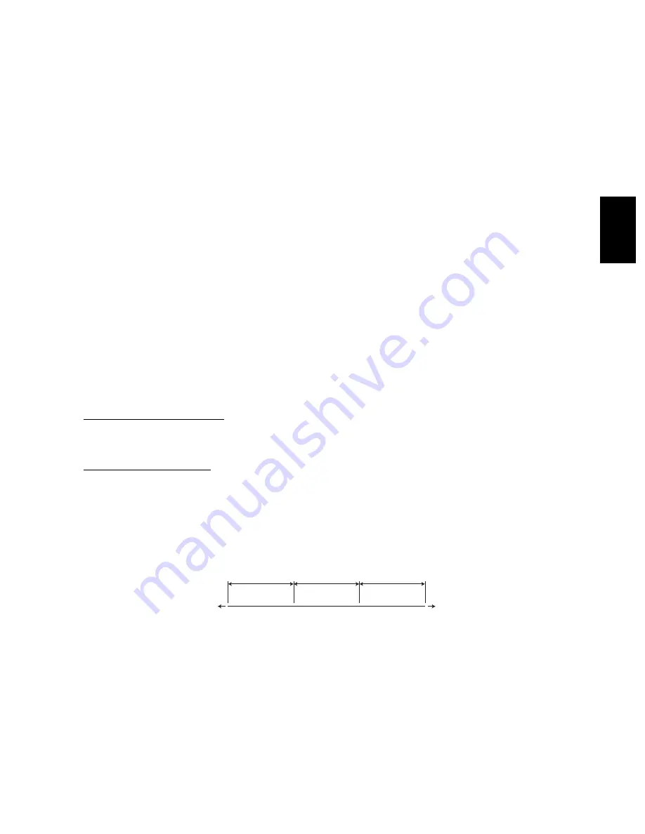
The adjustment code varies according to where blotched image and poor transfer occur. Select the
required adjustment code while referring to the following diagram.
Fig. 3-23
"220"
Approx. 11mm
Adjustment code
Leading edge
area of paper
Trailing edge
area of paper
"221"
"222"
Approx. 5mm
Содержание e-STUDIO163
Страница 6: ......
Страница 10: ...e STUDIO163 166 203 206 2005 2009 TOSHIBA TEC CORPORATION All rights reserved CONTENTS 4 ...
Страница 12: ......
Страница 142: ...e STUDIO163 166 203 206 2005 2009 TOSHIBA TEC CORPORATION All rights reserved ADJUSTMENT 3 58 ...
Страница 160: ...e STUDIO163 166 203 206 2005 2009 TOSHIBA TEC CORPORATION All rights reserved PREVENTIVE MAINTENANCE PM 4 18 ...
Страница 208: ...e STUDIO163 166 203 206 2005 2009 TOSHIBA TEC CORPORATION All rights reserved TROUBLESHOOTING 5 48 ...
Страница 230: ...e STUDIO163 166 203 206 2005 2009 TOSHIBA TEC CORPORATION All rights reserved POWER SUPPLY UNIT 7 4 ...
Страница 232: ...e STUDIO163 166 203 206 2005 2009 TOSHIBA TEC CORPORATION All rights reserved WIRE HARNESS CONNECTION 8 2 ...
Страница 236: ......
Страница 237: ......


