R-Engine-D
Chapter 3: Hardware
3-13
based
RD
can increase system efficiency and minimize CPU overhead in a 10BASE-T network. The
RD
with CS8900 provides a true full-duplex Ethernet solution, incorporating all of the analog and digital
circuitry needed for a complete C/C++ programmable Ethernet node controller.
High-Voltage, High-Current Drivers
The ULN2003 has high voltage, high current Darlington transistor arrays, consisting of seven silicon NPN
Darlington pairs on a common monolithic substrate. All channels feature open-collector outputs for sinking
350 mA at 50V, and integral protection diodes for driving inductive loads. Peak inrush currents of up to
500 mA sinking are allowed. These outputs may be paralleled to achieve high-load capability, although
each driver has a maximum continuous collector current rating of 350 mA at 50V. The maximum power
dissipation allowed is 2.20 W per chip at 25 degrees C (
°
C)..
ULN2003 is a sinking driver, not a
sourcing driver.
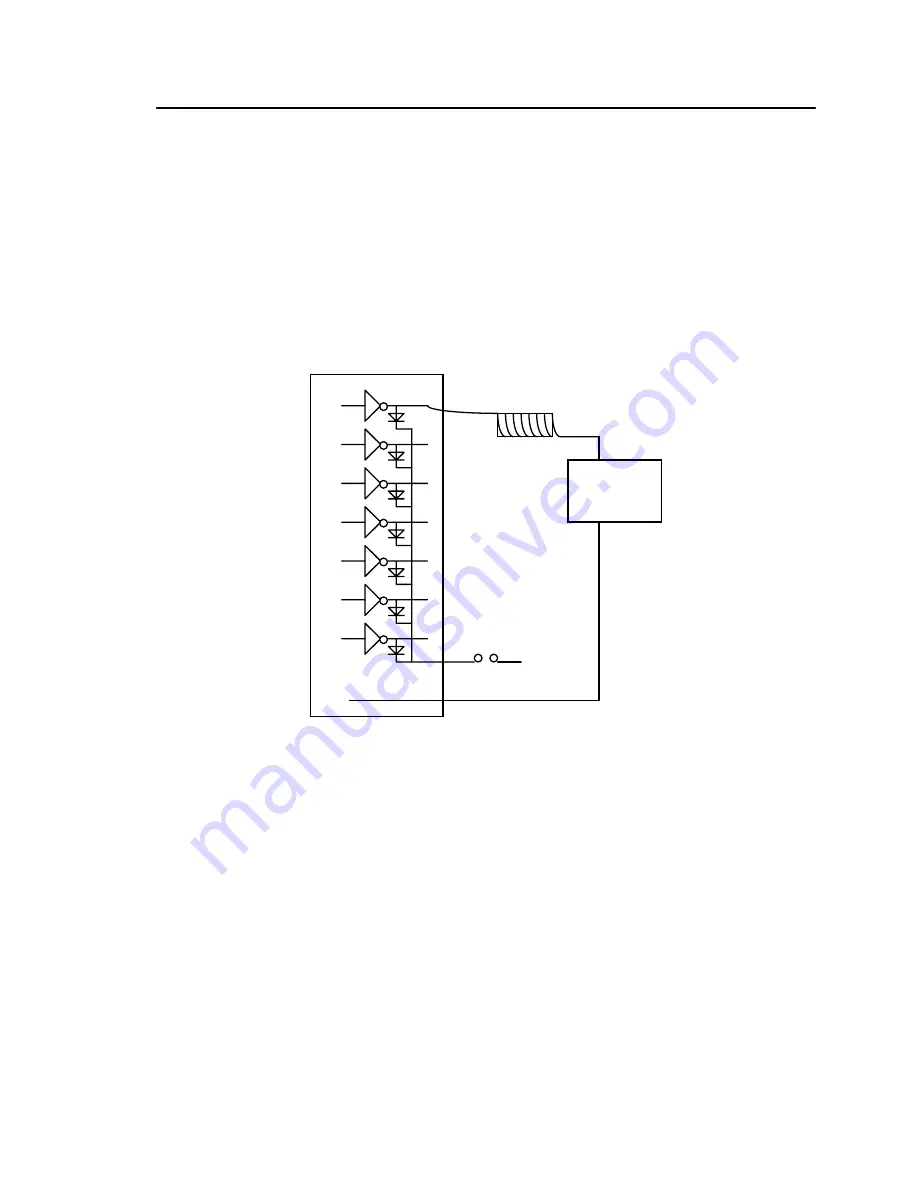
An example of typical application wiring is shown in Figure 1.1.
K
+12V
+12V
GND/SUB
GND/SUB
Power Supply
Solenoid
O1
ULN2003 TinyDrive
Figure 1.1 Drive inductive load with high voltage/current drivers.
By default the high voltage drivers are configured to sinking drivers, not sourcing, and for output. This
requires the common substrate be tied to GND and the K voltage diodes are tied to the highest voltage in
the system when driving inductive loads. The U29 socket is configured for sinking driver output only. The
common substrate is tied to ground by design, and the user can provide external voltage on K (routed to
J3.25) for inductive loads. For non-inductive loads K can be open (floating). The outputs of the U29
ULN2003A are routed to J3.27-32 and are driven by port 2 of the PPI (U5).
There are also two sockets at U10 and U30. By default they are sinking drivers for output. For the
S
INKING
driver configuration (default) this means that the common substrate are connected to the PCB
signal names VS and VS1 (do not be confused by the signal names on the schematic). These must be
connected to ground at the J3 header, thus J3.14 = J3.16 and J3.2 = J3.4. If inductive loads are being
driven, the user can provide external voltage on GK and GK1.
The U10 socket:
(1)
Can be sourcing output


