AWARD Setup Program
12-9
12.3.3 Chipset Features Setup
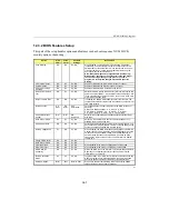
This part of the setup allows you to define chipset-specific options and features.
Option
BIOS
Default
Setup
Default
Possible
Settings
Description
SDRAM CAS Latency
Time
3
3
2, 3
For 100MHz SDRAM, set this option to 2 (clocks).
For 66MHz SDRAM, set this option to 3 (clocks).
DRAM Data Integrity
Mode
Non-
ECC
Non-
ECC
ECC,
Non-ECC
When set to ECC, allows auto-correction of the data read from
memory. It does not scrub the memory. The ECC error flags’
status register and the error pointer are updated if error correction
occurs in this mode.
When set to Non-ECC, no error checking or error reporting is
done.
System BIOS
Cacheable
Dis.
En.
En., Dis.
Selecting Enabled allows caching of the system BIOS ROM at
F0000h-FFFFFh, resulting in better system performance.
However, if any program writes to this memory area, a system
error may occur.
Video BIOS
Cacheable
Dis.
En.
En., Dis.
Selecting Enabled allows caching of the video BIOS ROM at
C0000h plus the VGA BIOS size, resulting in better video
performance. However, in any program writes to this memory
area, a system error may occur.
Video RAM Cacheable
Dis.
En.
En., Dis.
When Enabled, video memory region is cacheable. Some
offboard video card drivers may behave strangely; in such a case,
disable this option.
8 Bit I/O Recovery
Time
3
1
1, 2, 3, 4, 5, 6,
7, 8, NA
16 Bit I/O Recovery
Time
2
1
1, 2, 3, 4, NA
The I/O recovery mechanism adds bus clock cycles between PCI-
originated I/O cycles to the ISA bus. This delay takes place
because the PCI bus is so much faster than the ISA bus. These
two fields let you add recovery time (in bus clock cycles) for 16-bit
and 8-bit I/O.
Memory Hole At 15M-
16M
Dis.
Dis.
En., Dis.
You can reserve this area of system memory for ISA adapter
ROM. When this area is reserved, it cannot be cached. The user
information of peripherals that need to use this area of system
memory usually discusses their memory requirements.
Passive Release
En.
En.
En., Dis.
When Enabled, CPU to PCI bus accesses are allowed during
passive release otherwise the arbiter only accepts another PCI
master access to local DRAM.
Delayed Transaction
En.
En.
En., Dis.
The chipset has an embedded 32-bit posted write buffer to
support delay transactions cycles. Select Enabled to support
compliance with PCI specifications version 2.1.
AGP Aperture Size
(MB)
64
64
1, 8, ...256
This option determines the aperture size reserved to the
Accelerated Graphics Port (AGP).
Supervisor I/O Base
Addr.
190h
190h
190h, 290h,
390h
This option determines the base address for the Supervisor I/O
Register, which is used for such functions as power fail detection
and the watchdog timer.
Содержание TEK-CPCI 1003
Страница 15: ...TEK CPCI 1003 Technical Reference Manual 5 4 5 1 CONNECTOR LOCATION...
Страница 22: ...FEATURE DESCRIPTION 7 ONBOARD FEATURES...
Страница 51: ...TEK CPCI 1003 Technical Reference Manual 9 2 JUMPER LOCATION...
Страница 52: ...Setting Jumpers 9 3 JUMPER SETTINGS Table 1...
Страница 53: ...TEK CPCI 1003 Technical Reference Manual 9 4 JUMPER SETTINGS TABLE 2...
Страница 67: ...SOFTWARE SETUPS 12 AWARD SETUP PROGRAM 13 UPDATING THE BIOS WITH UPGBIOS 14 VT100 MODE...
Страница 95: ...C 1 C BOARD DIAGRAMS C 1 ASSEMBLY TOP DIAGRAM...


