


©2018
Rev 2.0
3
Communication Interfaces
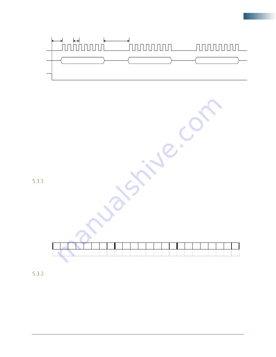
Figure 8. SPI timing.
As mentioned above, the SPI architecture limits the byte rate since after every byte transfer the input
and output SPI buffers need to be cleared and loaded respectively by the device SPI engine. Data is
transferred between the input buffer and internal register buffers. The time required to perform this
task is indicated by
𝑇
𝐵
, which is the time interval between the end of one byte transfer and the
beginning of another. The recommended minimum time delay for
𝑇
𝐵
is 1
𝜇𝑠
. The number of bytes
transferred depends on the register. It is important that the correct number of bytes is transferred
for the associated register, because once the first byte (MSB) containing the device register address
is received, the device will wait for the desired number of associated data bytes. The device will hang
if an insufficient number of bytes are written to the register. To clear a hung condition, the device
will need an external hard reset. The time required to process a command is also dependent on the
command itself. Measured times for command completions are typically between 50
𝜇𝑠
to 300
𝜇𝑠
after reception.
Writing the SPI Bus
The SPI transfer size (in bytes) depends on the register being targeted. The first byte sent is the
register address and subsequent bytes contain the data associated with the register. As data from
the host is being transferred to the device via the MOSI line, data present on its SPI output buffer
is simultaneously transferred back, MSB first, via the MISO line. The data returned is invalid for
configuration registers. The following figure shows the contents of a single 3-byte SPI command
written to the device. The Hardware Registers section provides information on the number of data
bytes and their contents for an associated register. There is a minimum of 1 data byte for each
register even if the data contents are “zeros”.
Figure 9. Example of a 3-byte write
Reading the SPI Bus
Data is simultaneously read back during an SPI transfer cycle. Requested data from a prior
command is available on the device SPI output buffers, and these are transferred back to the user
host via the MISO pin. To obtain valid requested data would require querying the
SERIAL_OUT_BUFFER, which requires 8 bytes or 64 clock cycles; 1 byte for the device register
(0x37) and 7 empty bytes (MOSI) to clock out the returned data (MISO). An example of reading the
device RF parameters (IF3 frequency) from the device is shown in the following figure.
T
S
T
B
T
C
8 Bit Command/ Reg. Address
Byte N (MSB)
Byte N-1 (LSB)
CLK
DATA
CS
23
15
7
0
Register Address
Byte 1
Byte 0