SIGNALCORE SC5309A Скачать руководство пользователя страница 41


Rev 2.0 | SC5309A & SC5310A 

Hardware Manual


SignalCore, Inc. 

SC5309A & SC5310A Hardware Manual 

The bulk transfer from the host to the device operates on a loopback with a data buffer of 8 bytes. 
When a device register is addressed, and upon completion of the register task, such as changing 
frequency, it will send back 8 bytes, which the host must read to clear the transfer buffers. Unlike 
the other interface methods, where only the required number of bytes needs to be sent for a given 
register, 8 bytes are needed for every USB bulk transfer. For example, if a configuration register 
requires only 4 bytes to be sent, these bytes will be the first of the 8 bytes and the last 4 bytes are 
zeros. The returned 8 bytes do not carry valid data for a configuration register. However, they do 
carry valid data for query registers.  


SPI Interface 

The SPI interface on the device is implemented using an 8-bit (single Byte) buffer for both the input 
and output, hence, it needs to be read and cleared by the device before consecutive bytes can be 
transferred to and from it. The process of clearing the SPI buffer and decisively moving it into the 
appropriate register takes CPU time, so a time delay is required between consecutive bytes written 
to or read from the device by the host. The chip-select pin (

𝐶𝑆

̅̅̅

) must be asserted low before data 

is  clocked  in  or  out  of  the  product. 

Furthermore,  pin 

𝐶𝑆

̅̅̅̅

  must be  asserted  low  for  the entire 

duration of a register transfer. 

Once a full transfer has been received, the device will proceed to process the command and de-
assert low the SRDY pin. The status of this pin may be monitored by the host because when it is de-
asserted low, the device will ignore any incoming data. The device SPI is ready when the previous 
command is fully processed and the SRDY pin is re-asserted high. It is important that the host either 
monitors the SRDY pin or waits for 500 

𝜇𝑠

 between register writes. 

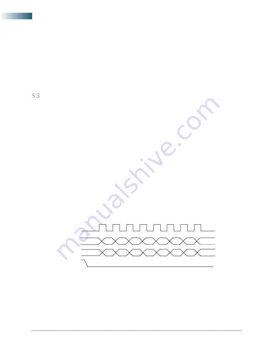
There are 2 SPI modes: 0 and 1. The default mode is 1, where data is clocked in and out of the device 
on the falling edge of the clock signal. In mode 0, data is clocked in and out on the rising edge. To 
select  mode  0,  pin  23  of  the  interface  connector  must  be  pulled  low  to  ground  as  the  device  is 
powered  on  or  as  the  reset  line  (pin  19)  is  toggled  low-high.  If  pin  23  is  pulled  high  or  left 
unconnected, mode 1 is selected.  


Figure 7. SPI Mode 1 shown. 

Register writes are accomplished in a single write operation. Register lengths vary depending on the 
register.  They  vary  in  lengths  of  2  to  8  bytes,  with  the  first  byte  sent  being  the  register  address 
followed  by  the  data  associated  with  that  register.  The  (

𝐶𝑆

̅̅̅

)  pin  must  be  asserted  low  for  a 

minimum period of 1 

𝜇𝑠

 (

𝑇

𝑆

, see 

Figure 8

) before data is clocked in, and must remain low for the 

entire register write. The clock rate may be as high as 5.0 MHz (

𝑇

𝐶

 = 0.2 

𝜇𝑠

), however, if the external 

SPI signals do not have sufficient integrity due to trace issues, the rate should be lowered.  

MSB

CS

MISO

MOSI

CLK

MSB

LSB

LSB

Содержание SC5309A

Страница 1: ...2018 SignalCore Inc All Rights Reserved Hardware Manual SC5309A SC5310A 2 5 GHz RF Downconverter www signalcore com...

Страница 2: ...l Connections 8 Device LED Indicators 10 Communication and Supply Connection 10 Mini USB Connection 11 Reset Button Pin Hole 12 3 Functional Description 13 Overview 13 The Signal Chain 14 The RF Input...

Страница 3: ...CE_CLOCK 28 Register 0x19 REFERENCE_DAC 29 Register 0x1A FREQ_PLAN_PARAM 29 Register 0x1B SYNTH_MODE 2 Bytes 30 Register 0x1C SYNTH_SELF_CAL 30 Register 0x1D USER_EEPROM_WRITE 31 Query Registers 31 Re...

Страница 4: ...the Device Via RS232 4 Reading from the Device Via RS232 5 PXI Express 5 Setting Up the PCI to Serial Bridge 5 Writing to the Device 6 Reading from the Device 6 6 Calibration 7 Calibration EEPROM Map...

Страница 5: ...CUSTOMER S RIGHT TO RECOVER DAMAGES CAUSED BY FAULT OR NEGLIGENCE ON THE PART OF SIGNALCORE INCORPORATED SHALL BE LIMITED TO THE AMOUNT THERETOFORE PAID BY THE CUSTOMER SIGNALCORE INCORPORATED WILL NO...

Страница 6: ...rdous materials must be explicitly declared Each of those materials and the categorical amount present in our products are shown below Lead Pb Mercury Hg Cadmium Cd Hexavalent Chromium Cr VI Polybromi...

Страница 7: ...EMS HARDWARE AND OR SOFTWARE UNANTICIPATED USES OR MISUSES OR ERRORS ON THE PART OF THE USER OR APPLICATIONS DESIGNER ADVERSE FACTORS SUCH AS THESE ARE HEREAFTER COLLECTIVELY TERMED SYSTEM FAILURES AN...

Страница 8: ...l SignalCore products in their original antistatic bags Remove the product from its packaging and inspect it for loose components or any signs of damage Notify SignalCore immediately if the product ap...

Страница 9: ...C5310A Hardware Manual SignalCore Inc 8 SC5309A SC5310A Hardware Manual Front Interface Indicators and Connectors The SC5309A is a PXIe based RF downconverter with all user I O located on the front fa...

Страница 10: ...eper cleaning is necessary use lint free swabs and isopropyl alcohol to gently clean inside the connector barrel and the external threads Do not mate connectors until the alcohol has completely evapor...

Страница 11: ...rectly Off No supply or supply error Table 2 Active Indicator LED Color Description Green An external interface port has accessed the device Red Input supply voltage exceeded Off No current interface...

Страница 12: ...9 RX MOSE RX DTE for RS232 or MISO for SPI 30 SRDY This pin is serial ready for SPI Mini USB Connection This is a mini USB Type B connector for USB communication with the device using the standard USB...

Страница 13: ...le is the reset button which is only available on the SC5310A Using a pin to lightly depress this momentary action push button switch will cause a hard reset to the device putting it back to its defau...

Страница 14: ...ly Module The downconverter has a maximum of three conversion stages The first converted intermediate frequency IF stage is called IF1 whose signal is converted from the RF input signal The second con...

Страница 15: ...n referred to as the signal chain which is shown on the system block drawing in Figure 4 The RF Input All RF connectors are high quality female stainless steel SMA types rated to 18 GHz of operation T...

Страница 16: ...ier is enabled Turning on this amplifier is recommended to improve the signal to noise dynamic range DRSNR when expected signal levels are lower than 30 dBm The typical maximum gain of the downconvert...

Страница 17: ...to optimally reject leakages inside their passband or within their filter slope This LO1 leakage will mix with the converted IF1 signals or with LO2 to produce higher order unwanted in band spurs that...

Страница 18: ...especially for those frequencies that are less than the BW of BPF0 The Third mixer and IF3 Path The third IF IF3 is tunable from 5 MHz to 100 MHz as LO3 is tuned from 220 MHz to 420 MHz in 5 MHz steps...

Страница 19: ...the gain should be shifted to the RF input path of the device before the mixer The RF pre amplifier should be enabled if necessary and or RF attenuation reduced The IF3 attenuator is then used to adju...

Страница 20: ...base reference whenever an external reference source is not used When an external reference is selected as the base clock by enabling the device to phase lock to it the effect only occurs when the pre...

Страница 21: ...normally fixed at 3 32 GHz by it may be set via the frequency plan to tune between 3 1 GHz and 3 45 GHz in 5 MHz frequency steps LO2 drives the second mixer of the signal chain Its frequency is indire...

Страница 22: ...ed on board their voltages are regulated and actively filtered to keep noise to a minimum Thus these downconverters are tolerant to dirty external power supplies 8V 5V 3 3V 5V To LO SignalChain Module...

Страница 23: ...rpret the incoming data leaving the device in a stalled state The total number of bytes is the sum of the register address 1 Byte and its corresponding data bytes For example to set the RF frequency v...

Страница 24: ...N_PARAM 0x1A 7 0 Frequency word Hz 7 0 15 8 Frequency word Hz 15 8 23 16 Frequency word Hz 23 16 31 24 Frequency word Hz 31 24 39 32 Frequency word Hz 39 32 47 40 Frequency word Hz 47 40 55 48 Set to...

Страница 25: ...1 WO Unused 7 Set to zeros 7 0 RO Read back byte 8 Read 1 byte back is required for PXIe and RS232 Register 0x10 RF_FREQUENCY This register tunes the device to the input RF frequency Bytes written 8...

Страница 26: ...read 1 Bits Type Name Width Description 0 W Frequency word 1 0 Disables the RF amplifier 1 Enables the RF amplifier 7 1 W Unused 7 Set to zeros 7 0 R Read back byte 8 Read 1 byte back is required for...

Страница 27: ...1 0 Selects the IF2 filter 0 1 Selects the IF2 filter 1 custom option 2 W invertSpectrum 1 0 Not spectral inversion 1 IF3 spectrum inverted w r t RF 3 W Bypass_rf_conversion 1 0 RF is converted to IF...

Страница 28: ...will change the state of the RF amplifier to provide the best device configuration to meet the input parameter requirements 4 3 W linearMode 2 0 Best signal to noise SNR least linear 1 Better SNR suf...

Страница 29: ...ead back byte 8 Read 1 byte back is required for PXIe and RS232 Register 0x17 DEVICE_STANDBY This register sets either the entire device or sections of the device into standby mode Placing a section i...

Страница 30: ...back byte 8 Read 1 byte back is required for PXIe and RS232 Register 0x19 REFERENCE_DAC This register makes adjustments to the 10 MHz TCXO accuracy via DAC to its tuning port Bytes written 4 Bytes re...

Страница 31: ...r synthesizers It also enables or disables faster tuning of the YIG based oscillator of LO1 Bytes written 2 Bytes read 1 Bits Type Name Width Description 1 0 WO Loop Gain 2 0 Low loop gain improves ph...

Страница 32: ...eturn while others do not need any For example the register GET_DEVICE_PARAM 0x30 returns the RF Frequency IF1 Frequency IF3 Frequency etc the data returned depends on the parameter value of the instr...

Страница 33: ...ce parameter to query from the device Bytes written 2 Bytes read 8 Bits Type Name Width Description 3 0 W Parameter 1 0 Returns current RF frequency 1 Current IF1 frequency 2 Current IF2 frequency 3 C...

Страница 34: ...ad 8 Bits Type Name Width Description 7 0 W Unused 7 Set to zeros 0 R Pll status LO1 sum 1 The summing PLL of LO1 1 R Pll status LO1 crs 1 The coarse tuning PLL of LO1 2 R Pll status LO1 fine 1 The fi...

Страница 35: ...ainEnable 1 19 R autoGainEnable 1 Auto calc of gain enabled default 0 Software gain calculation used 1 Gain can be read back from device less accurate 63 20 R Invalid data 29 Ignore Register 0x23 GET_...

Страница 36: ...ress Bytes written 4 Bytes read 8 Bits Type Name Width Description 15 0 W Address 16 Starting EEPROM address 23 16 W Unused 8 Zeros 63 0 R Data 64 8 bytes of data LSB is the byte at the start address...

Страница 37: ...eros zeros SC Gain SC Config Frequency parameter values Frequency parameter values are returned in the first 7 bytes with the last byte padded with zeros The least significant bit LSB is 1 1000 Hertz...

Страница 38: ...ial number as an unsigned 32 bit integer Byte 4 contains the interface as represented in the following table Table 8 Interface ID Bit Description 0 PXI PXIe 1 USB 2 SPI 3 RS232 7 4 Undefined Revision...

Страница 39: ...2018 SignalCore Inc All Rights Reserved Section 2 Communication Interfaces and Calibration...

Страница 40: ...1 Frequency is sent in 1000th of Hertz so the data that represents the frequency is 2 500 000 000 000 milli Hertz 2 This number can be represented by a 64 bit unsigned long and in Hexadecimal is 0x 0...

Страница 41: ...re pin must be asserted low for the entire duration of a register transfer Once a full transfer has been received the device will proceed to process the command and de assert low the SRDY pin The stat...

Страница 42: ...s depends on the register being targeted The first byte sent is the register address and subsequent bytes contain the data associated with the register As data from the host is being transferred to th...

Страница 43: ...15200 upon reset or power up Data bits The number of bits in the data is fixed at 8 Parity Parity is 0 zero Stop bits 1 stop bit Flow control 0 zero or none Only 3 wire RS232 is required since hardwar...

Страница 44: ...icates with the onboard microcontroller serially The interface on the bridge chip resides at offset addresses between 0x00 and 0xFF from BAR0 which is memory mapped A kernel level driver for the opera...

Страница 45: ...device register The first byte sent is the device register address followed by the most significant byte of the register s associated data When a device register is fully written that is all its data...

Страница 46: ...cies 5 10 15 100 in MHz 0x510 21 84 Float_32 IF3 relative gain response to the IF set for absolute RF gain measurement 0x72C 30 120 Float_32 Relative If3_atten 1 1 30 dB 1 dB step 0x7A4 30 120 Float_3...

Страница 47: ...dB IF2 Filter setting is 0 Inverted spectrum set to 0 RF amplifier disabled set to 0 IF frequency is set at user specific setting or defaults to 50 MHz RF is tuned to the list frequencies 5 10 20 90...

Страница 48: ...h we shall call _ 6 The gain for this configuration is calculated using 2 3_ 1 3 1 If the current device temperature is different from the calibration temperature the gain correction due to temperatur...

Страница 49: ...ware Manual Revision Table Revision Revision Date Description 1 0 8 10 18 Initial Release 1 1 2 26 19 Added feature to signal path register 16 Changed figure 6 to reflect latest conversion path implem...

Отзывы: